PCB Design: Practices and Principles
When designing my PCBs, I take into consideration a number of things. Here are some of the considerations I make.
Manufacturer tolerances
When designing your PCB, make sure to design it within manufacturer tolerances. If you are unsure of what manufacturer you plan on using, it is wise to find a couple and use the loosest tolerance so that you have the option later on to choose a specific manufacturer. Most manufacturers have the same tolerances, however, it pays to always double check.
Snap grid and spacing
When designing a PCB layout, understanding where and at what distance components should be arranged is important. Utilizing the snap grid and keeping component separation consisten makes for a clean looking PCB. Additionally, spacing components such that a soldering iron can be used or using hand-soilder friendly footprints can be beneficial for prototype PCBs or boards that you may expect to be modifying in the future.
Clearly label with silkscreen
When spacing out components on the PCB, adjust the placement to prevent overlap in silkscreen. Make sure all reference designators are visible and unambiguous in their placement.
Trace Width (for DC applications, low frequency, and power distribution)
The width of your traces will play a large part in how much current can flow through them. Select trace width based on application and current/resistance requirements. Below is a table of IPC recommended track widths for a 1 oz copper PCB. The values are calculated based on the current required to raise the temperature of the trace by 10 degrees celsius.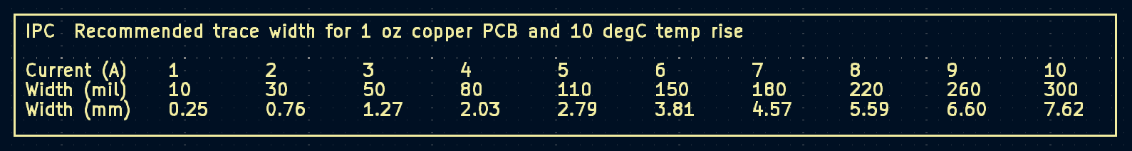
Trace Spacing
The spacing of your traces depends on the purpose of the traces. In applications where signals are being sent, it is best to follow the 3W rule, where you space two parallel traces 3 time the trace width apart. This will reduce interference (crosstalk) between the two traces.
Trace Bends
When you need to make a bend in a trace, it is important to keep in mind the type of signal the trace is carrying. For low frequency signals and applications where trace length or resistance is not a concern, a 90 degree (a) turn is acceptable, and can sometimes give the PCB a unique look. Typically, a 45 degree miter (b) would be employed for general use in digital and analog signaling as it reduces overall trace resistance (shorter length) and has better high-speed signaling characteristics. For high-voltage power or radio-frequency signals, a round bend (c) would be used as it has the best high-speed characteristics, maintains a consistent characteristic impedance, and, for high-voltage, does not have any sharp corners for charges to build up on.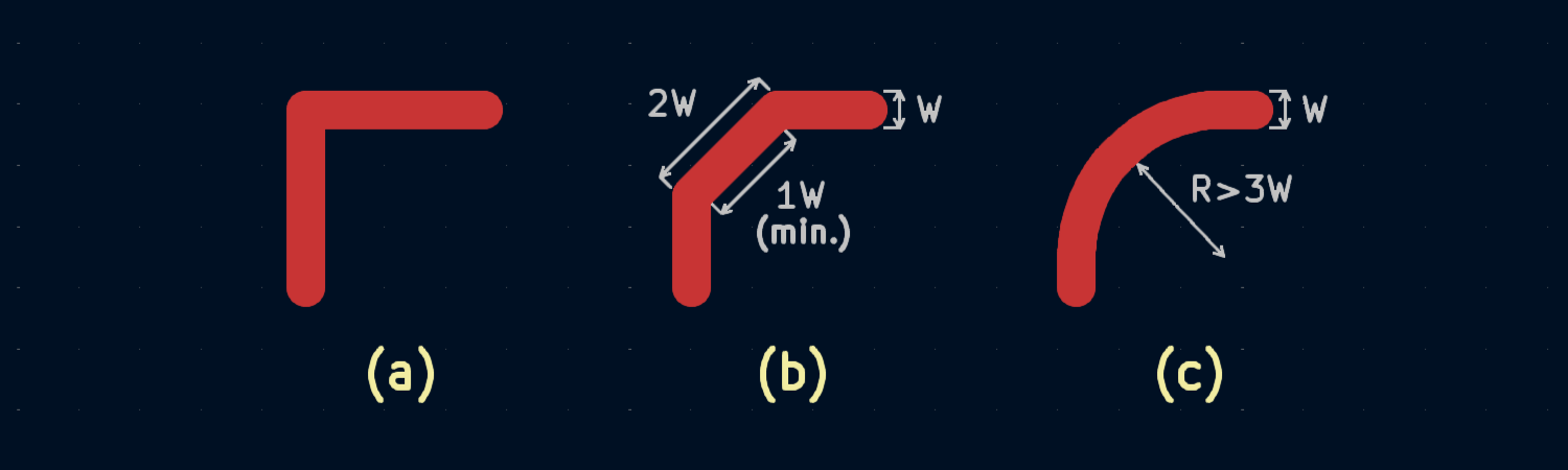
Trace Junctions
Avoid junctions of more than 3 traces. When making a 3-way junction, avoid acute angles. Acute angles create signal reflections at higher frequencies, and generate etchant “acid” traps during manufacturing. When choosing a junction, the 90 degree (a) is perfectly acceptable for general use, but as the signal speed gets faster, the mitred (b) or ‘Y’ junction (c) may improve high-speed signal characteristics and signal integrity.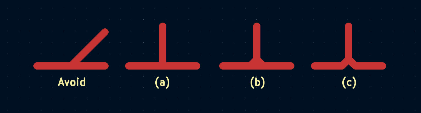
Place Decoupling Capacitors Close to ICs
When you design a PCB layout for a schematic containing decoupling capacitors for ICs, always place the decoupling capacitor as close to the IC power input pin as possible, and connect it directly to a ground plane using a short trace or via.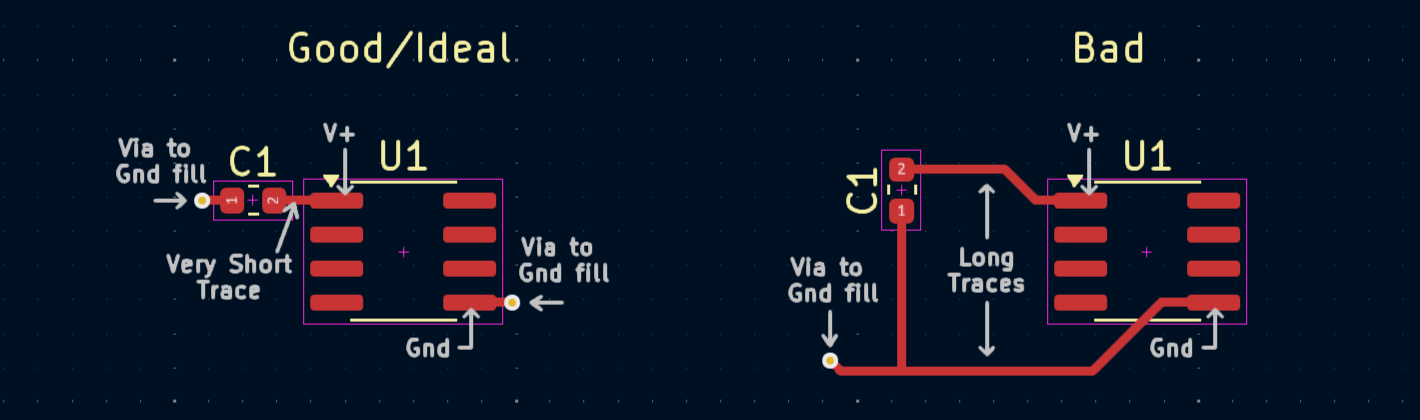
Power and Ground Planes
If you are designing a PCB with 4 or more layers, the two inner layers should be a copper layer for power and ground. This will reduce the number of traces needed to distribute power, reduce EMI, and create a shorter path to both power and ground through vias.
Power and Signal Distribution
There are three methods for power distribution: single point source, star source, and multipoint source. Each has their strengths and weaknesses. Below is a table to summarize:
Information & figures to be added.
Differential Pairs
When designing a PCB layout containing differential pairs, keep the trace lengths the exact same. Most EDA CAD softwares automatically maintain the differential pair length, but in some cases you may need to enable that function.
SMD Thermal paths and Reflow Considerations
When soldering surface mount components using solder paste and a hot air station (or reflow oven), the surface tension of molten solder will automatically align surface-mount devices (SMDs) on their pads. This however can cause issues where the thermal relief on pads may create colder areas on the pad where solder may solidify faster. In the case of pads with traces connecting from top and bottom (a), the component may

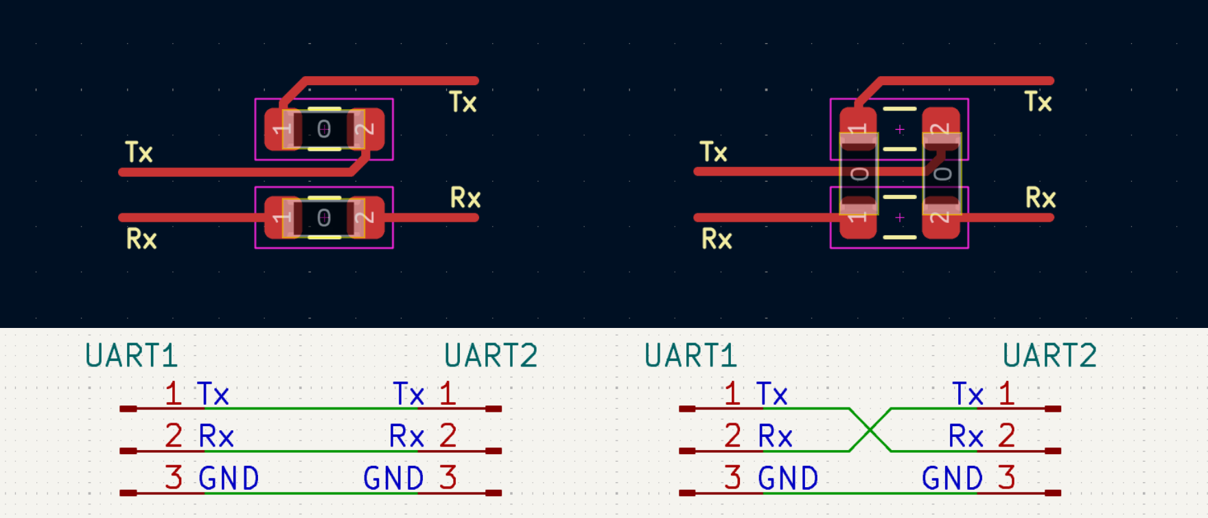
Serial RX/TX Poka-yoke (UART, SPI, RS232)
When working with serial connections that require a crossover, such as two serial devices where the Rx of one is connected to the Tx of the other (and vice versa) a poka-yoke method can be used. The method shared here is one that I personally prefer.
Poka-yoke Origin
- Poka-yoke (ポカヨケ; [poka joke]) is any mechanism in a process that helps an equipment operator to avoid mistakes and defects by preventing, correcting, or drawing attention to human errors as they occur. Poka-yoke was originally baka-yoke, but as this means "fool-proofing" (or "idiot-proofing") the name was changed to the milder poka-yoke.
In the event an error is made in the design, this method of footprint layout can ensure no matter the Tx/Rx arrangement between devices, one can still recover from the error by changing the way the jumpers are soldered to the board.