Schematic Drawing: Practices and Principles
In an effort to make the schematics I draw consistent and tidy while containing all necessary information, I use the following practices.
A must watch video that goes over some of what is discussed below, but also goes into more detail on some important topics. Overall, it encompases the essence of good schematic design and I like it a lot. A Great Video
Utilize the snap grid
When using any EDA CAD software, turn on the snap grid and set it to a dimension that will remain constant throughout your drawings. Consistency in your schematics is key to ensuring your schematics remain consistent, clear, and readable.
Signal and Voltage Flow
A schematic layout should have the signal path going from left to right. With feedback signals going right to left, as they are "feeding back". It is best to have the higher voltage connections close to the top of the page, and lower voltage connections close to the bottom of the page. Power connection symbols should always be vertical, with positive voltages pointing up and negative voltages (including ground) pointing down.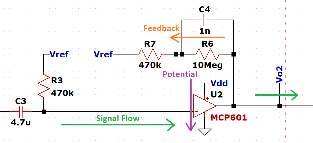
Design on standard paper size
Design your schematic so that they are readable on a standard printer size paper like A4 or 8.5”x11”. This allows them to be easily printed. For larger circuits, you may need to design the schematic over multiple pages to keep your drawings organized and readable.
Text Font
Text on the schematic should be uniform, simple, and every character should be easily legible at all font sizes. For that reason fonts that are very vector-like, with straight lines, unambiguous, are best. Make sure the font you choose has good spacing to prevent symbols such as underscores from being covered by other lines in the schematic such as symbols or wires. Common fonts to use are Arial, Consolas, or Tahoma. In addition to font, always make text for components, nets, labels, notes, etc. ALL CAPS.
Text placement
Adjust the placement of the text associated with a symbol to not overlap other text and to make the text orientation consistent. It is good practice to have the designators and values on either side (or occasionally on the top and bottom) of horizontally oriented components and on the right side above and below vertically oriented components as shown below.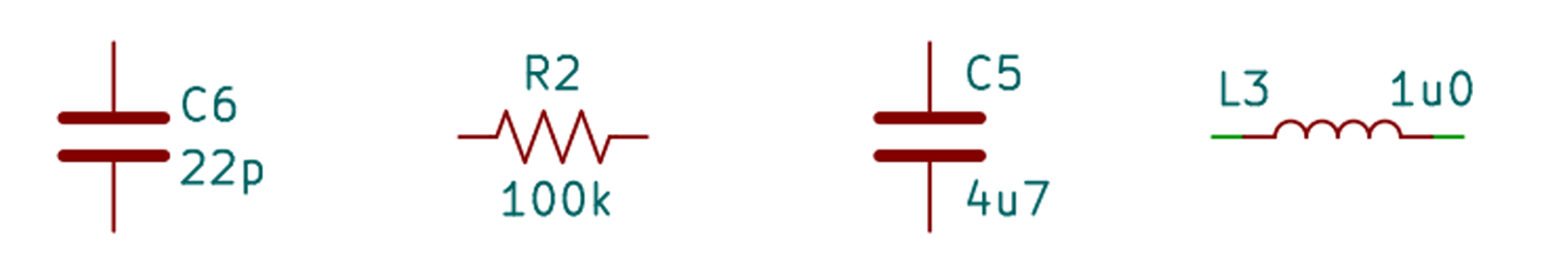
Defining Junctions
Draw a dot at every junction and make all junctions T’s. Do not draw 4-way cross junctions. With two lines crossing, one vertical the other horizontal, the only way to know whether they are connected is whether the junction dot is present.
The reason this is done is to prevent ambiguity in the event of generation loss. An example of generation loss may be the schematic is physically printed and scanned multiple times, or a screenshot is taken and compressed, then sent through email. When the image quality of the schematic is lost, the dots used to indicate a junction may fade, disappear, or reappear in places they shouldn’t.
When drawing or reading schematics, the general rule is if two lines cross then they are never connected, even if after some reproduction or compression artifacts it looks like there maybe is a dot there. By making all junctions Ts with dots, all crossing lines are therefore different nets without dots. In addition to this, never use an arc to indicate one net crossing over another. This is an old method and considered bad practice.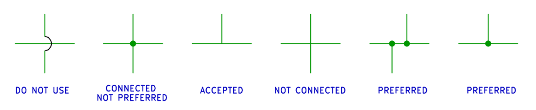
Keep symbols consistent
Always use the same symbol for the same device. For instance, there are multiple ways to draw different types of resistors, capacitors, logic gates, etc. When drawing these symbols, choose one symbol for the device and keep it consistent throughout your project's schematics.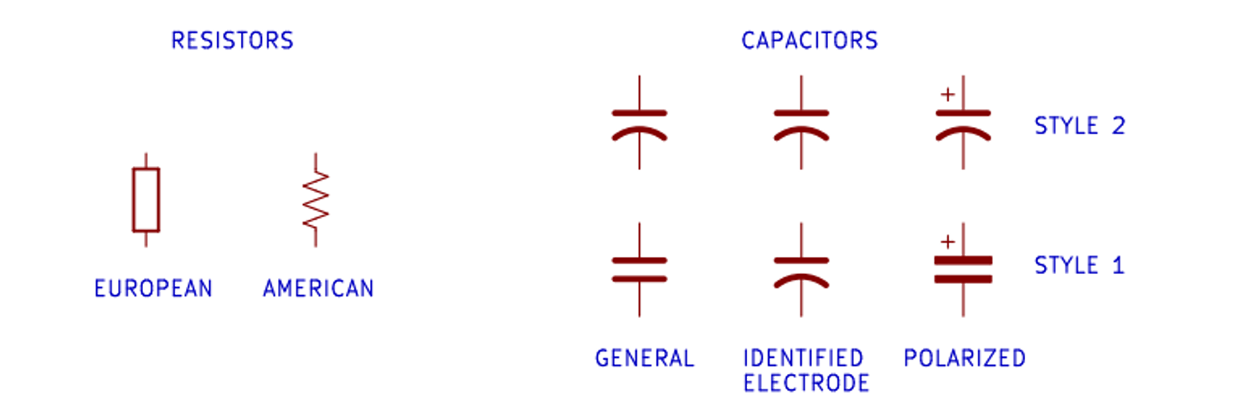
Break it down into blocks
Break down your design into blocks based on functions, signal types, voltage domains, etc. Doing this will make designing on multiple pages easier, troubleshooting quicker, and overall improve organization. Adding a block diagram to the first page of your schematic package will also improve organization and searchability.
An example of this would be to draw a power supply design on one schematic page, then perhaps an amplifier on the other, so on and so forth.
Common circuit topologies
When drawing known building blocks and sub-circuits, draw them as they are commonly known and ensure they are recognizable. An example of this would be a common emitter amplifier. The drawing on the left is easily recognizable as a common emitter amplifier, while the drawing on the right is hardly recognizable as the common emitter topology.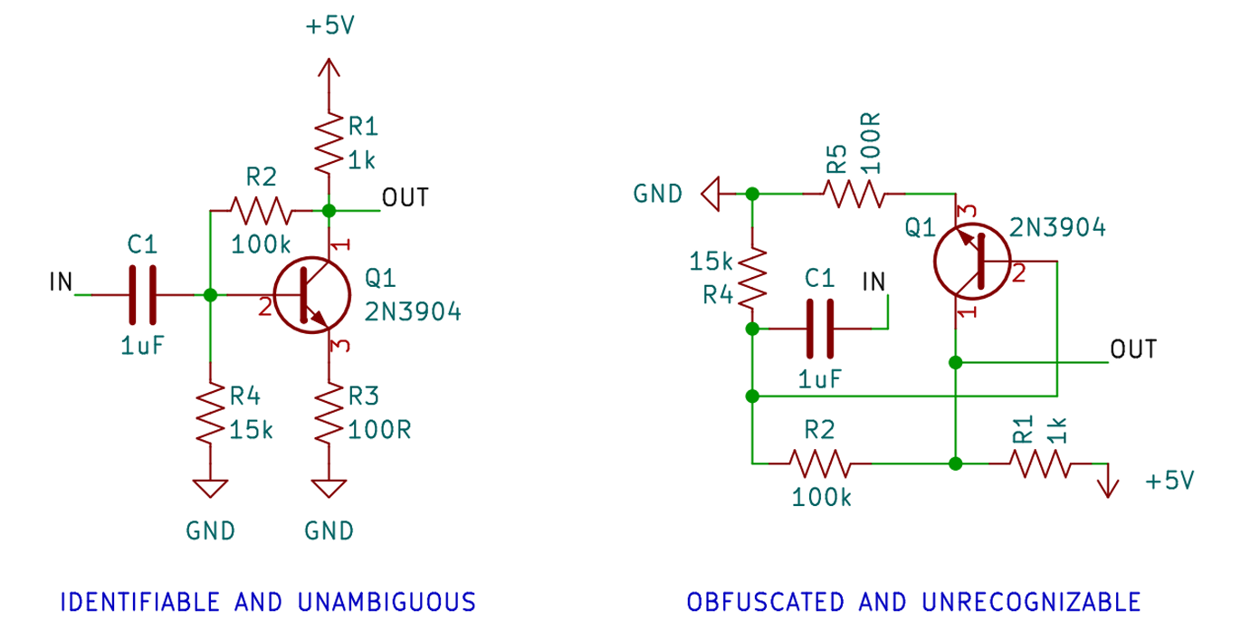
Draw pins according to function
Show pins of ICs in a position relevant to their function. Following the signal path and layout, when drawing an IC, have the voltage inputs at the top, grounds and negative voltages at the bottom, inputs on the right, and outputs on the left. Physical pin order layouts obfuscate the circuit, so it is best to avoid them.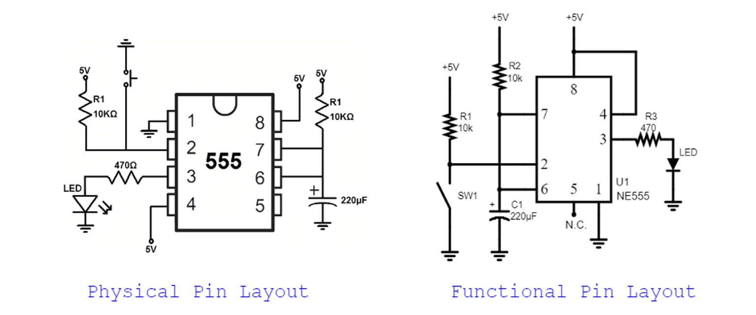
Spacing
Leave enough space between pins to make the pins readable and consistent. A good rule of thumb for this is to leave enough space so you can add resistors on top of eachother with room for text (this is particularly helpful when adding resistor arrays).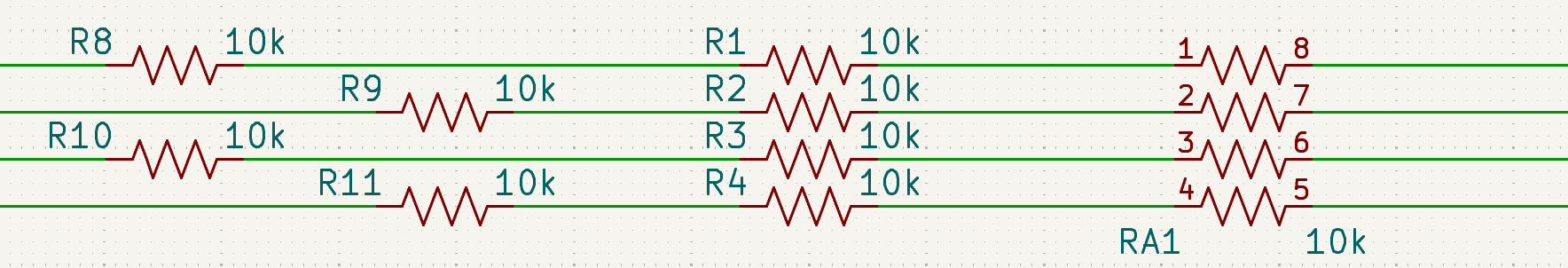
Wires and busses
When designing a schematic with parallel logic or wires that should be grouped together, use a bus where possible. A bus will group the wires and show as one thick wire on the schematic (depending on EDA). This saves space, and increases readability. Avoid crossing busses if possible as this can lead to ambiguities.
Net names
Placed directly on a “wire” connection, explicit net names are used to clarify the purpose of a signal, or label a specific type of signal. A common use for net names is to name the signals on connector pins. In most EDA CAD software, nets are global, so they can be used across multiple pages of a schematic to define connections.
Use ports/labels for distant connections
When designing schematics that have one or more connections spanning the entire page, it is better and more organized to use a label instead of drawing a wire across the entire page to connect the two points. In the case of a multi-page schematic, labels are necessary. Use direct wires where possible, but use labels to complete the less than direct connections.
Decoupling capacitor placement
Because of the purpose of decoupling capacitors, they need to be physically placed very close to the part. On a schematic, it is best practice to place decoupling capacitors by their IC power pins. This makes the intent of the component clear, and can prevent mistakes later in the PCB design process. It also makes troubleshooting a lot easier!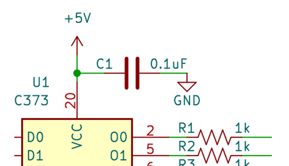
Standard component values
When designing a circuit in a simulation or calculating values, your components may have specific and non-standard values. An example of this could be the requirement of a 1.0634 kOhm resistor, which does not exist on the market. So unless it is a critical value, not using standard values will only make manufacturing and parts sourcing extremely difficult or impossible.
Standard values for resistors, capacitors, and inductors most commonly follow the E-Series of preferred numbers, details of which are explained in the IEC 60063:2015 standard. You can also go to the E-Series of preferred numbers - Wikipeda page to read further.
For fuses, standard values follow the Renard series of preferred numbers, more of which can be found in the ISO 3:1973 standard or at Renard Series - Wikipeda.
Value notation and tolerance
While giving capacitors, inductors, and resistors values, use metric system international (SI) suffix letters in place of the decimal point. As schematics get routinely photocopied or otherwise optically reproduced, decimal dots can disappear after a few generations. To prevent any chance of errors this convention was adopted. As a bonus, it makes values shorter and quicker to read. SI suffix letters used are shown below.
| Letter | SI Unit | 10^ | Used for | Example Case |
|---|---|---|---|---|
| p | Pico | -12 | Capacitors | 33p for 33pF, 8p1 for 8.1pF |
| n | Nano [1] | -9 | Capacitors, Inductors | 2n2 for 2.2nF, 39n for 39nH |
| u | Micro | -6 | Capacitors, Inductors | 4u7 for 4.7uF, 10u for 10uH |
| m | Milli | -3 | Capacitors, Inductors, Resistors | 1m for 1mF, 3m3for 3mF |
| R | Ohm [2] | 0 | Resistors only | 37R5 for 37.5 Ohms, 220R for 220 Ω |
| k | Kilo | 3 | Resistors | 2k2 for 2.2k Ohms, 22k for 22kΩ |
| M | Mega | 6 | Resistors | 3M3 for 3.3 M Ohms |
Notation
- Using nano (n) for capacitors and inductors is not typical in industry. It is more common to use micro (u) and pico (p). Ex. 2200p for 2.2n or 0u8 for 800n.
- The "R" is only used for resistors and is used in place of the decimal. Capacitors and inductors are indicated with their units for sizes larger than what is commonly occurring within the schematic such as a 1 F capacitor.
When writing out the component value, use 3 characters (including the SI letter) to denote a 5% tolerance, use 4 characters to denote 1%, and use 5 characters for 0.5/0.1%. Ex. 1M0 for 1M Ohms 5%, 4u70 for 4.7uF 1%, 2k210 for 2.21k Ohms 0.1%.
Component tolerances
When designing a circuit, most passive components will follow the same tolerances, such as using 1% resistors across the entire circuit. Instead of indicating the tolerance of each component at the component, it is better to leave an engineering note on the drawing that states a default tolerance for a component type, then when you deviate from that tolerance you can add the tolerance value next to the component value.
Reference Designators
Reference designators are used to uniquely identify components within a circuit. A reference designator consists of a letter (or two) to indicate the type of component followed by a number to identify the specific component.
Make sure reference designators are visible, clear, and at the components side in the same orientation as all other reference designators. Most EDA CAD softwares have default reference designators, and the ability to add your own. Common reference designators can be found in the table below
| Designator | Description |
|---|---|
| R | Resistor, All kinds |
| RA | Resistor Array |
| C | Capacitor, All Kinds |
| CA | Capacitor Array |
| D | Diode, All kinds (including LED) |
| TVS | Transient Voltage Suppression Diode |
| L | Inductor, All Kinds (Excluding transformer) |
| T | Transformer |
| FB | Ferrite Bead |
| F | Fuse |
| Q | DiscreteTransistor |
| U | Integrated Circuits (Including Voltage Regulators, microcontrollers, and SoCs) |
| SW | Switch, Button |
| K | Relay |
| BAT | Battery Clip/Connection |
| J | Jack (Least movable connector of a connector pair) |
| JP | Jumper Connector (Link on Board) |
| P | Plug (most-movable connector of a connector pair) |
| A | Sub-module or PCB assembly |
Multi part packages
Multi part packages such as Quad Op Amps (4 op amps in one chip) or a hex inverter (6 inverters in one chip) may show up in schematics as U2A, U2B, etc. Make sure that all of the parts get “packaged” into the minimum number of IC packages required. If there are parts that aren’t being used, such as 5 of the 6 inverters being used in a hex inverter, consult the datasheet of the part to determine whether to pull unused pins low, high, or to leave them unconnected. Doing so can prevent the possibility of interference, crosstalk, or oscillations from occurring.
Part orientation
When drawing parts on a schematic such as an Op Amp, make sure not to flip the orientation in such a way that it is less commonly perceived. In the case of most op amps, they are drawn with the non-inverting input above the inverting input.
Do Not Populate (No-Pop) Option
Most EDA's have an option in their schematic editors to define a component as "Do Not Populate" (or No-Pop) for short. This option will allow the designer to keep a component in the design, but inform the manufacturer that the component is not needed to be soldered on to the PCB. One application of this option is to add multiple different footprints for one component -- say a PCB has an op-amp that can be ordered as a DIP-8 package or an SOIC-8 package. Depending on lead times and/or component availability, it helps to have both footprints on one's PCB to have the option to order either package of op-amp and not need to order different PCB's.