With my University Degree complete, I had much more free time to work on my superheterodyne reciever. Armed with more knowledge than my 2025 self, I decided it was worth redesigning most of it. Beginning with the frontend amplifier, I decided to try the cascode amplifier once again.
Cascode Configuration
Because I wanted to make the amplifier lower noise while maintaining dynamic range and linearity, I opted to use a BFR193 as my common emitter transistor, and a standard MMBT3904 as my common base transistor.
Because the BFR193 has a +30dBm IP3 at an Ic of 30 mA, I decided to keep the collector current high at 20 mA. Because of both manmade and solar noise, the lower HF bands such as 3.5 MHz, 7 MHz and 14 MHz won't benefit from low noise amplifiers. The audible difference of an amplifier with a 10 dB noise figure (NF) and 3 dB NF would be inaudible.
However, because the BFR193 is a low noise and high $f_T$ transistor, it should be plenty fine for my applications.
Design and Simulation
To design the amplifier, I decided to take a break from re-writing all my hand calculations every time I wanted to make a change, so I put together a simple MATLAB script (for GNU Octave) that calculates the values needed.
The script is not refined, but it was enough to get everything going: cascode.m
The circuit was put together in LTspice and an ac analysis was run.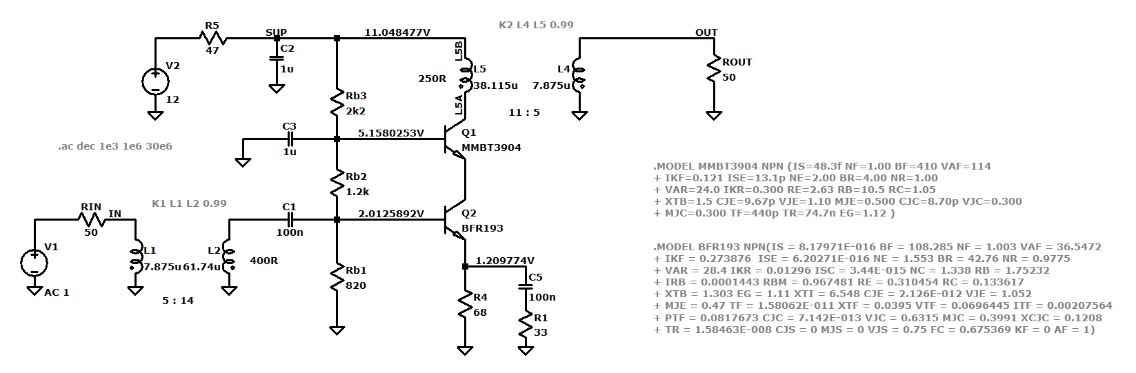
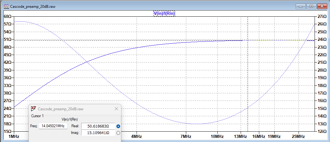
The gain was simulated to be around 21 dB, and the input impedance was close to 50 ohms with a slight reactive component to it. The benefit of using a high $f_T$ BJT as the common emitter transistor is the input and output capacitances are very small even with relatively high gain.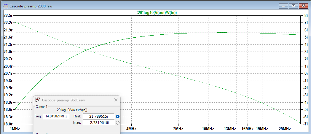
Because a Cascode amplifier presents itself as a current source at the common base transistors collector, a loadline match is necessary for the output. I chose to go with a 250 ohm load at the collector, which is easy to match to a 50 ohm output using a transformer.
I am using Fair-Rite 5943000901 43-mix toroids to wind the transformers, which are quite small meaning I need to use 30 AWG wire and keep the number of total turns low enough they fit on the core. Both input and output transformers are a manageable 5:14 turns and 11:5 turns respectively. I opted to use a partial bifilar winding on both transformers to better couple the primary and secondary.
Building the Amplfier
To build the amplifier I designed a single-layer SMD only PCB that I could easily etch. I challenged myself to make the board as compact as possible. The result was a 20mm x 30mm board.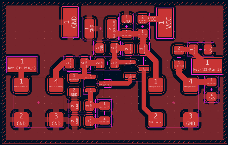
I then exported the design as an SVG and printed off the mirrored board onto some glossy paper for toner transfer. The toner transfer was successful as well, resulting in a well masked board.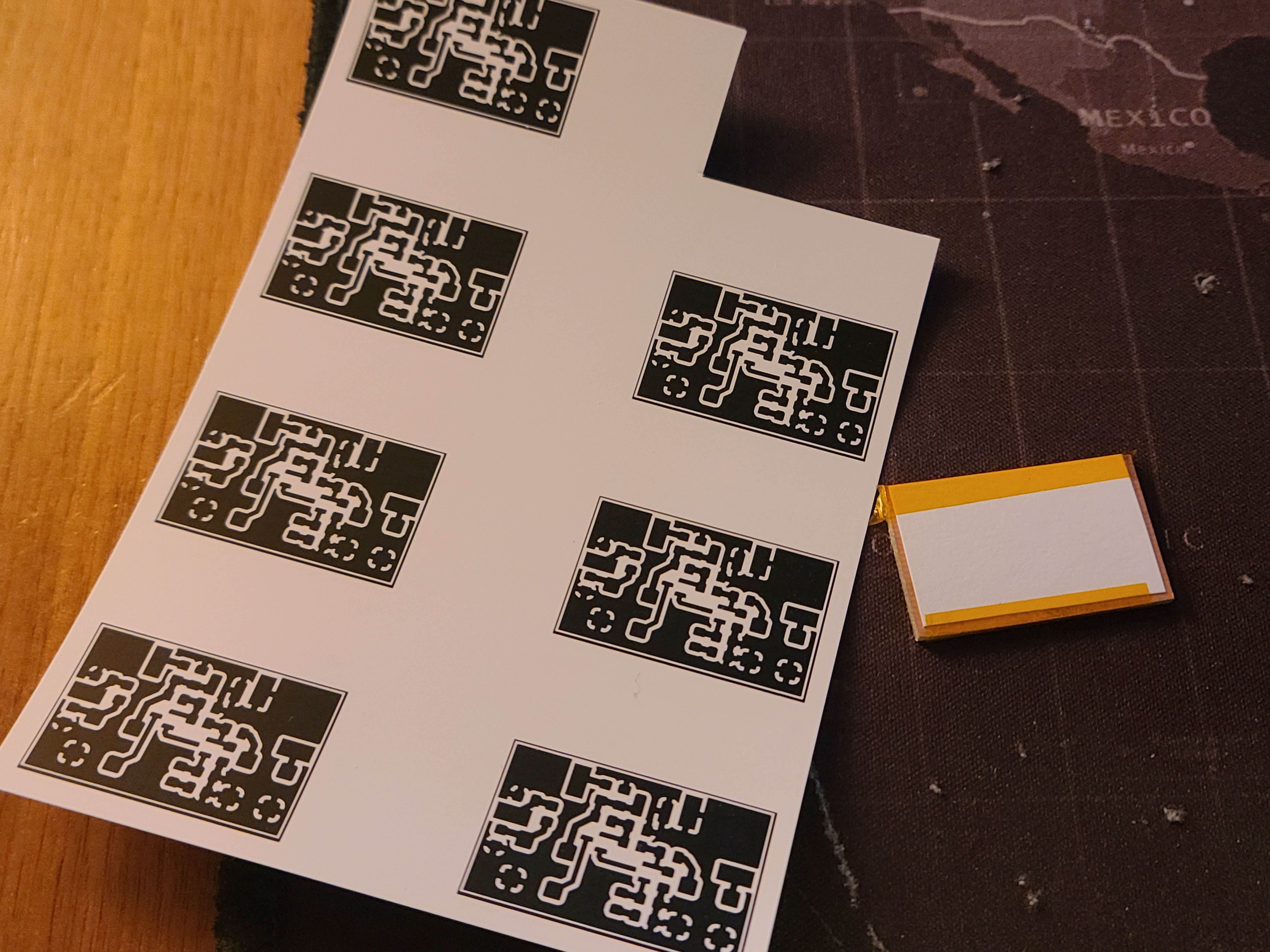
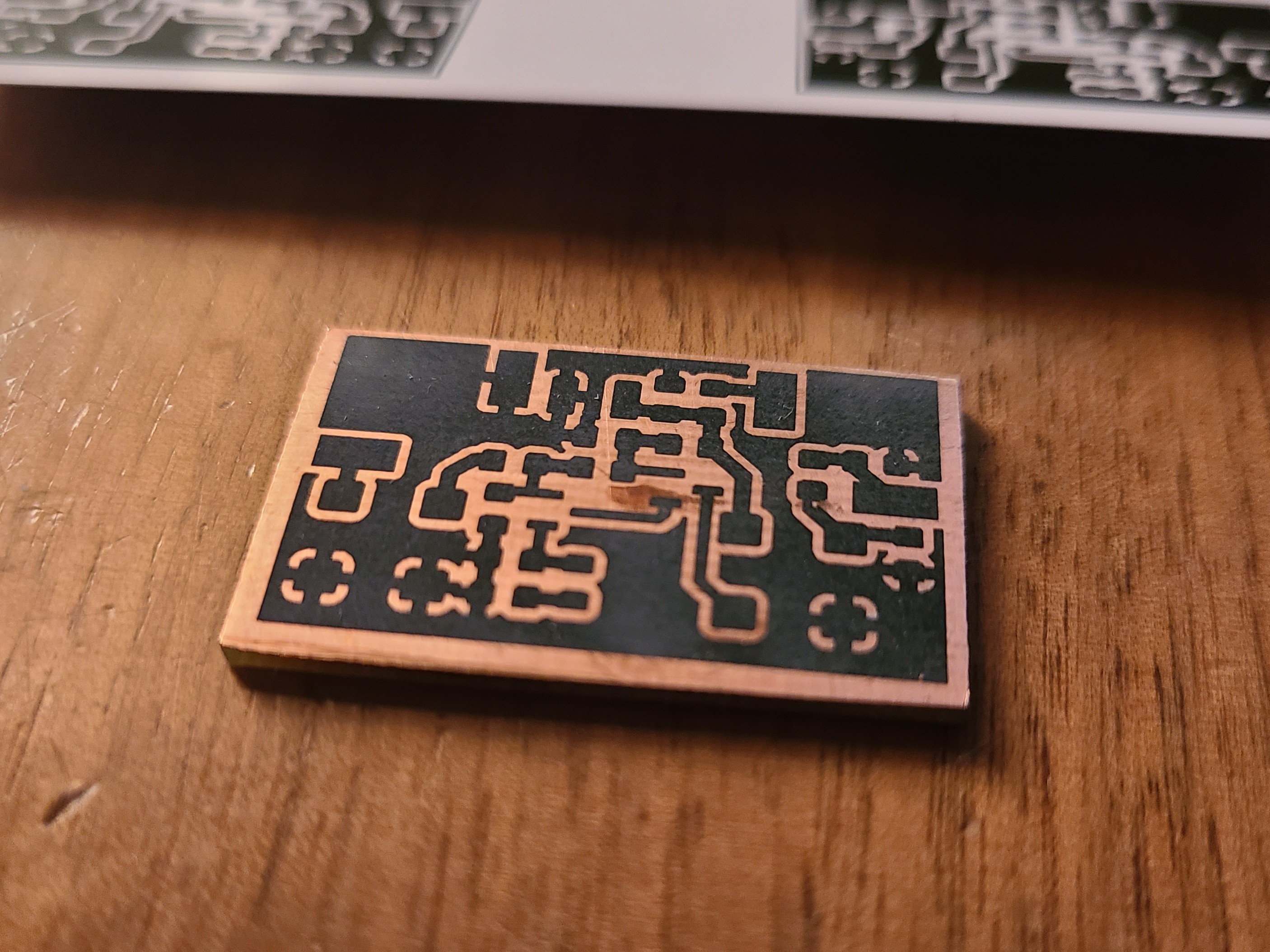
Once the toner transfer, I etched the board in some ferric chloride etchant.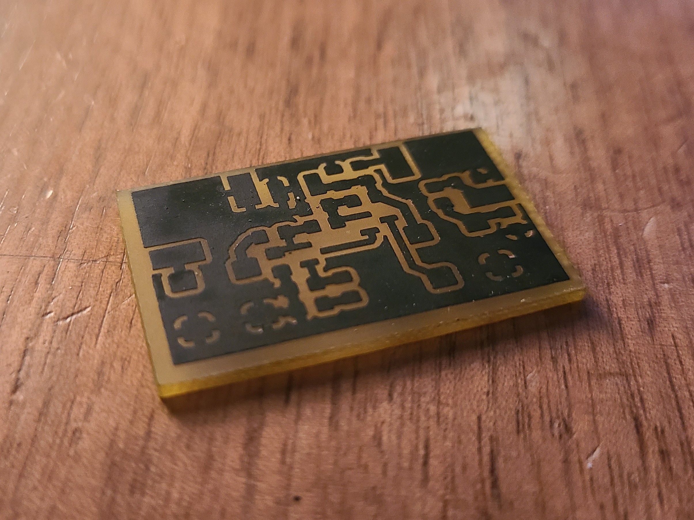
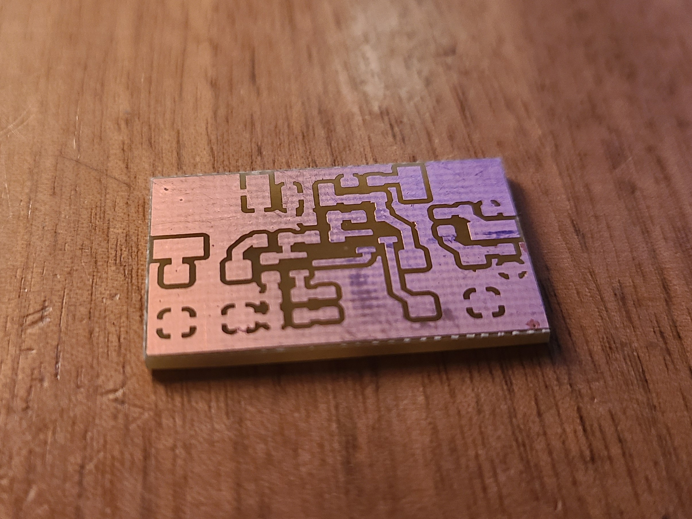
With the PCB etched, it was ready to be populated with components. The transformers were hand wound using two different color 30 AWG wire. In the PCB design I included pads to allow for a simple pi attenuator, but I ended up soldering a 0 ohm jumper and not including any attenuation.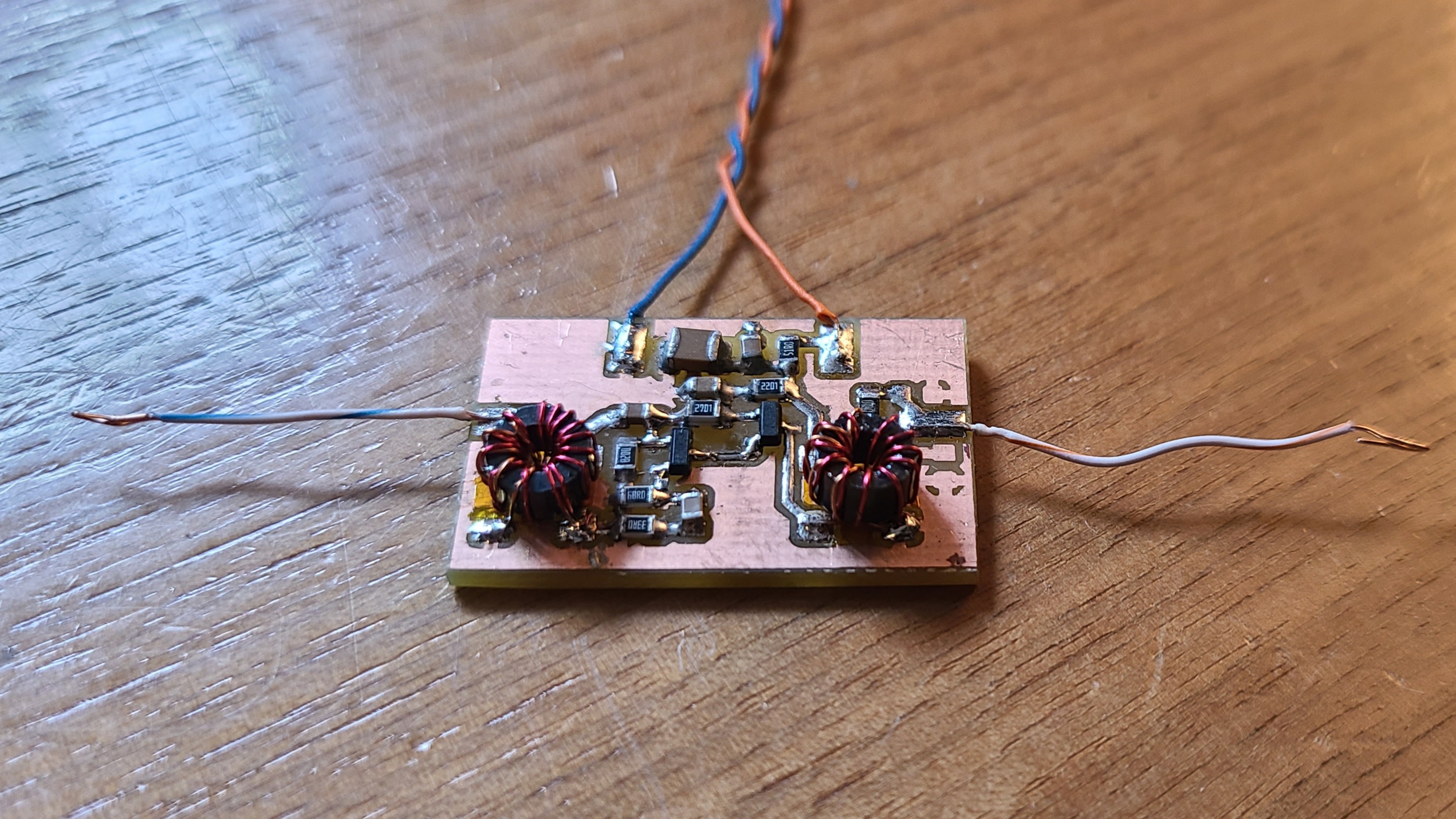
Testing
To test the amplifier, I used a NanoVNA-F V2 with some unconventional probes that I have less confidence in than some of my chinese probes. I made sure to calibrate the VNA at the end of the probes, but any change in position would have most likely affected it. I also used a 20 dB pad at the second port of the VNA to protect the VNA from any high amplitude signals.
The results of the shoddy test still confirmed the amplification and general impedance match lined up with the simulation.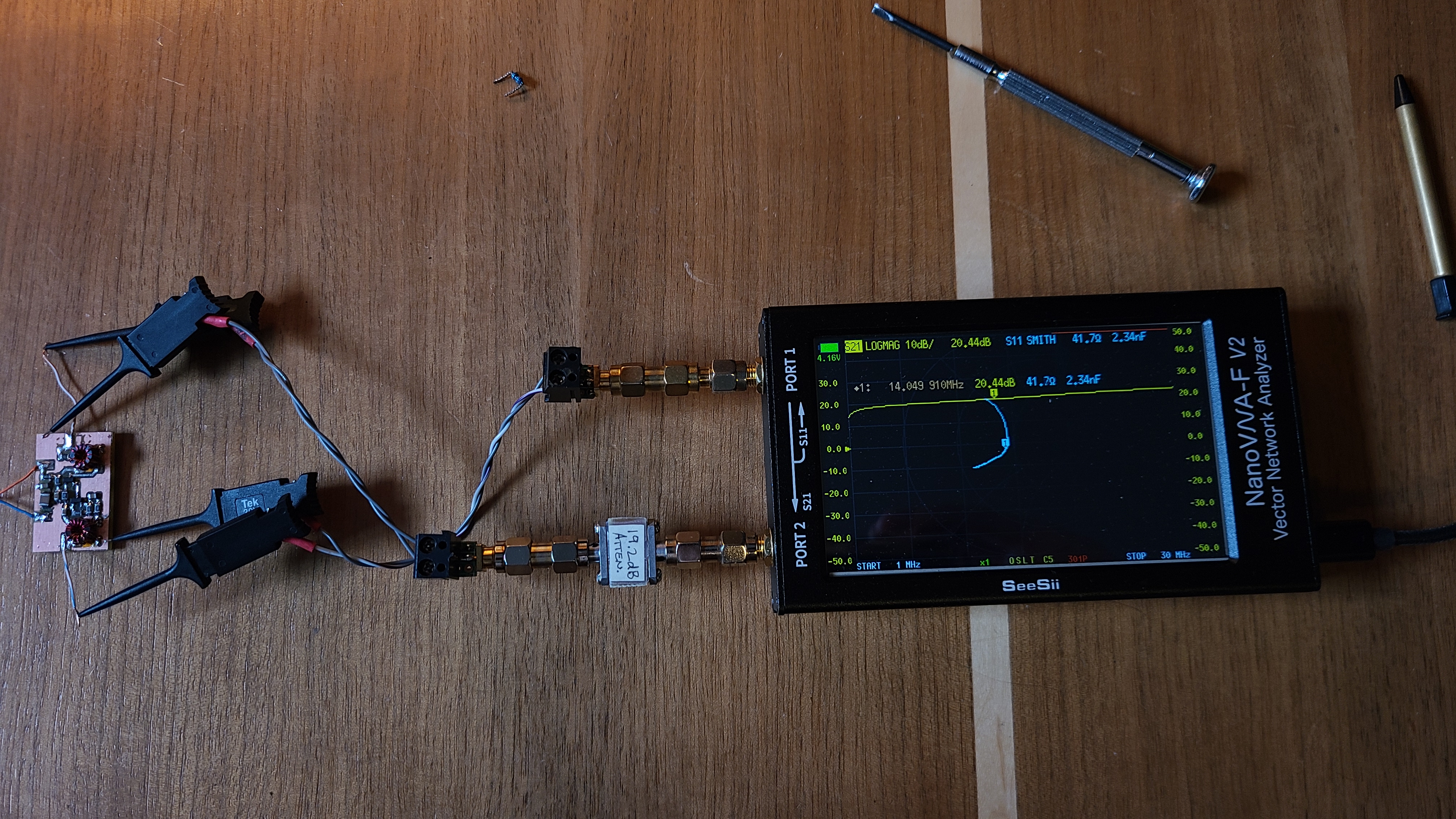
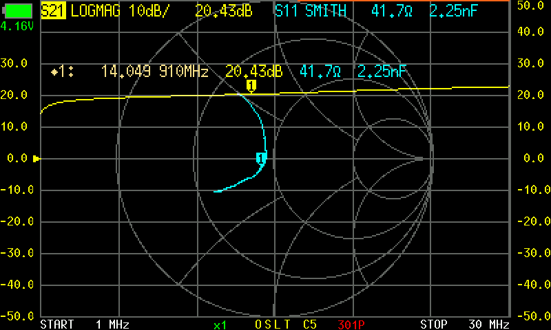
The gain was consistent at 20.43 dB, and input impedance was close to 50 ohms. The additional capacitance was likely the test setup having been repositioned after calibration.