The previous cascode design was insufficient, so I redesigned it with much better results.
Amplifier Design
Like the previous design, I opted to use the cascode configuration. The main difference in this design from the last is that I chose to use only 2N3904 BJTs.
While conducting some research, I found a paper by Vojtěch Janásek on the Design of ultra low noise amplifiers. In this paper, Vojtěch tested various generic BJT's and discovered the 2N3904 had a lower noise at Ic=1.3 mA (as compared to the BC549). Though the 1.3 mA metric is specific to an improvement compared to the BC549, I still opted to design my cascode around it.
A note on the paper
Equation 3 in the paper describes how to properly calculate the optimal collector current for low noise operation. For low source resistances the base spreading resistance rbb is addeed with the source resistance Rs to calculate Ic(opt). In the case of my circuit, I transformed my Rs from 50 ohms to 1220 ohms. With these values, I later (after building this circuit) calculated my Ic(opt) to be 270 uA.
In the future, I would either (a) lower my source impedance, or (b) decrease my collector current, to achieve better results.
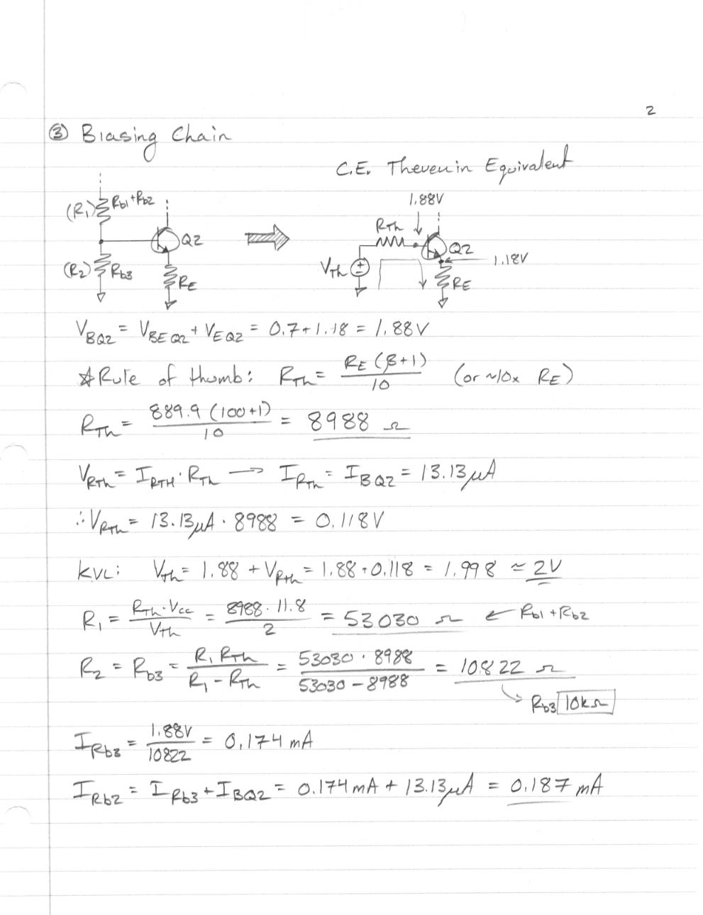
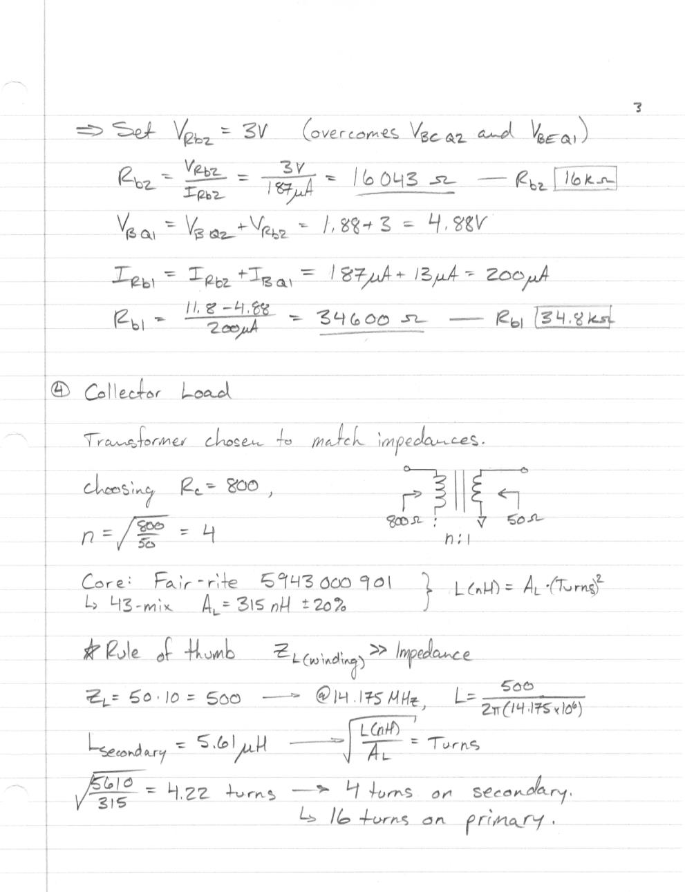
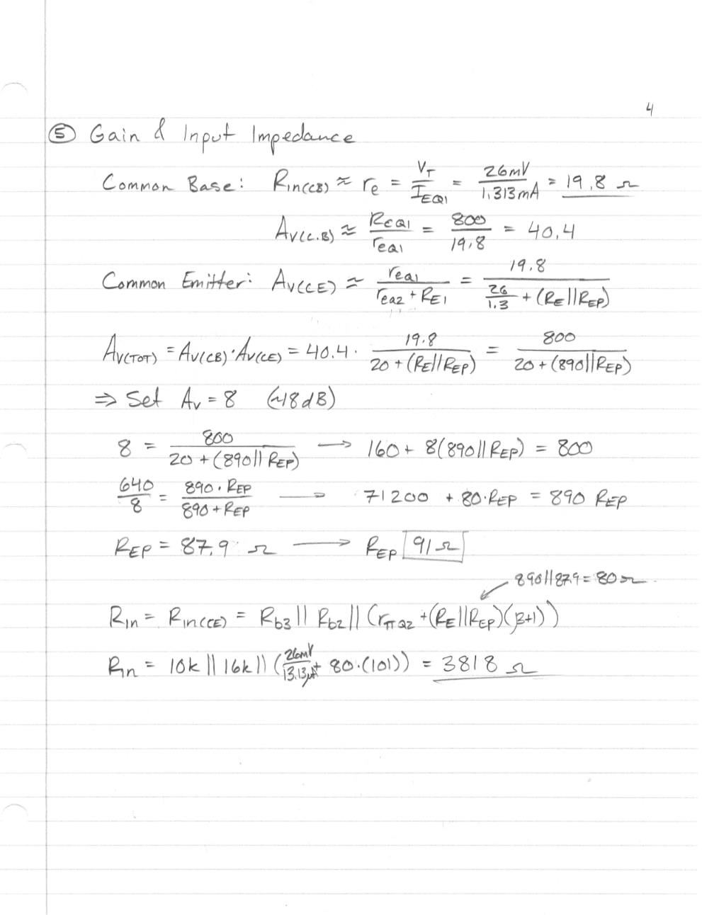
The calculations I made to design the cascode are shown in the PDF below. Expand to view Cascode Hand Calculations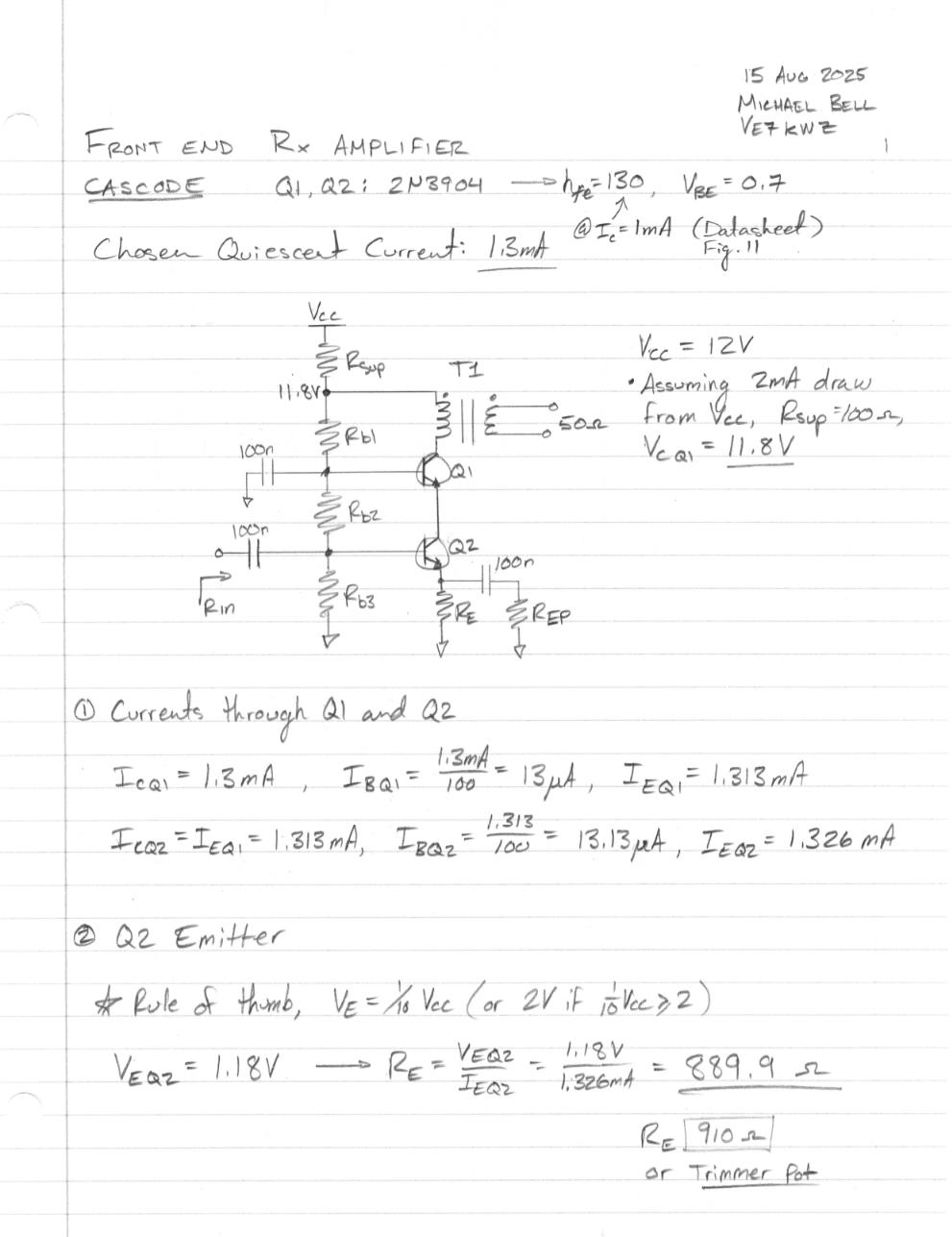
Simulation
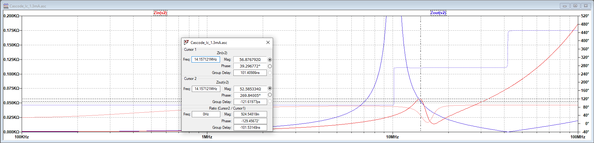
After calculating values, I created an LTSpice simulation of the amplifier. Below is the schematic, and measurements.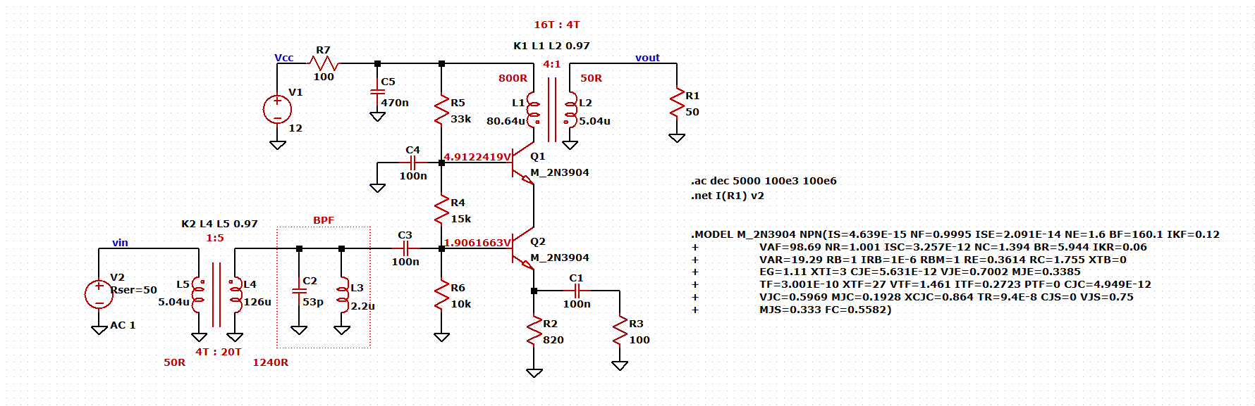
The output impedance result was very unexpected, as I thought my calculations were correct in using a 4:1 transformer to bump the impedance from my specified 800 ohms down to 50 ohms. This makes me believe I don't quite understand the concept of impedance transformers in amplifiers. At the end of this post I included modified spice simulations that fixes this issue, and the result is a 16:1 transformer believe it or not!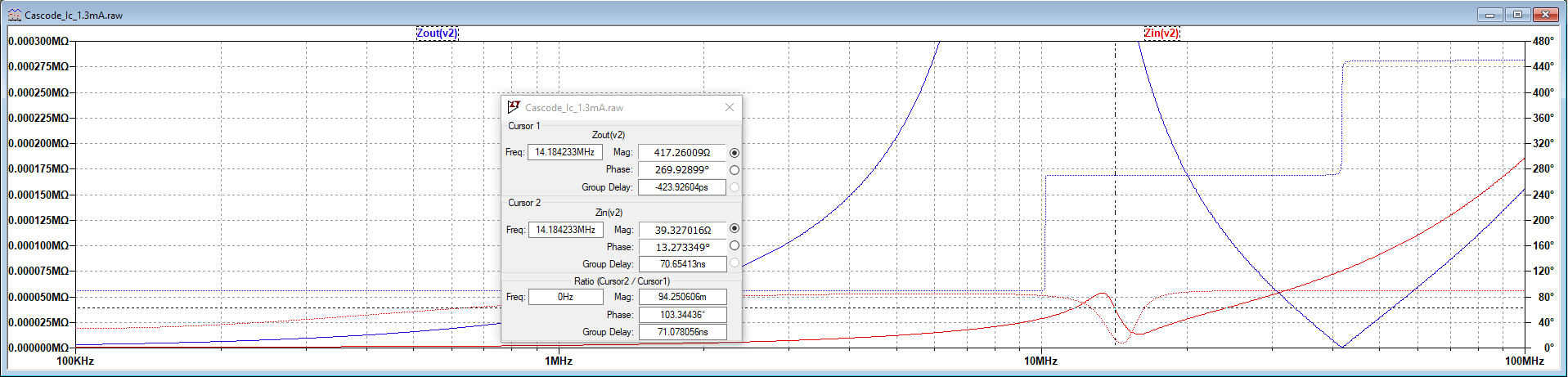
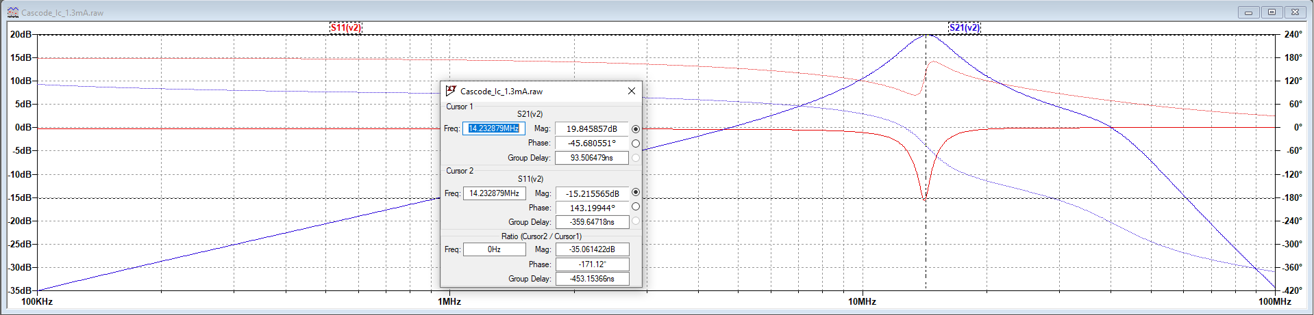
The gain provided by this amplifier turns out to be around 20dB.
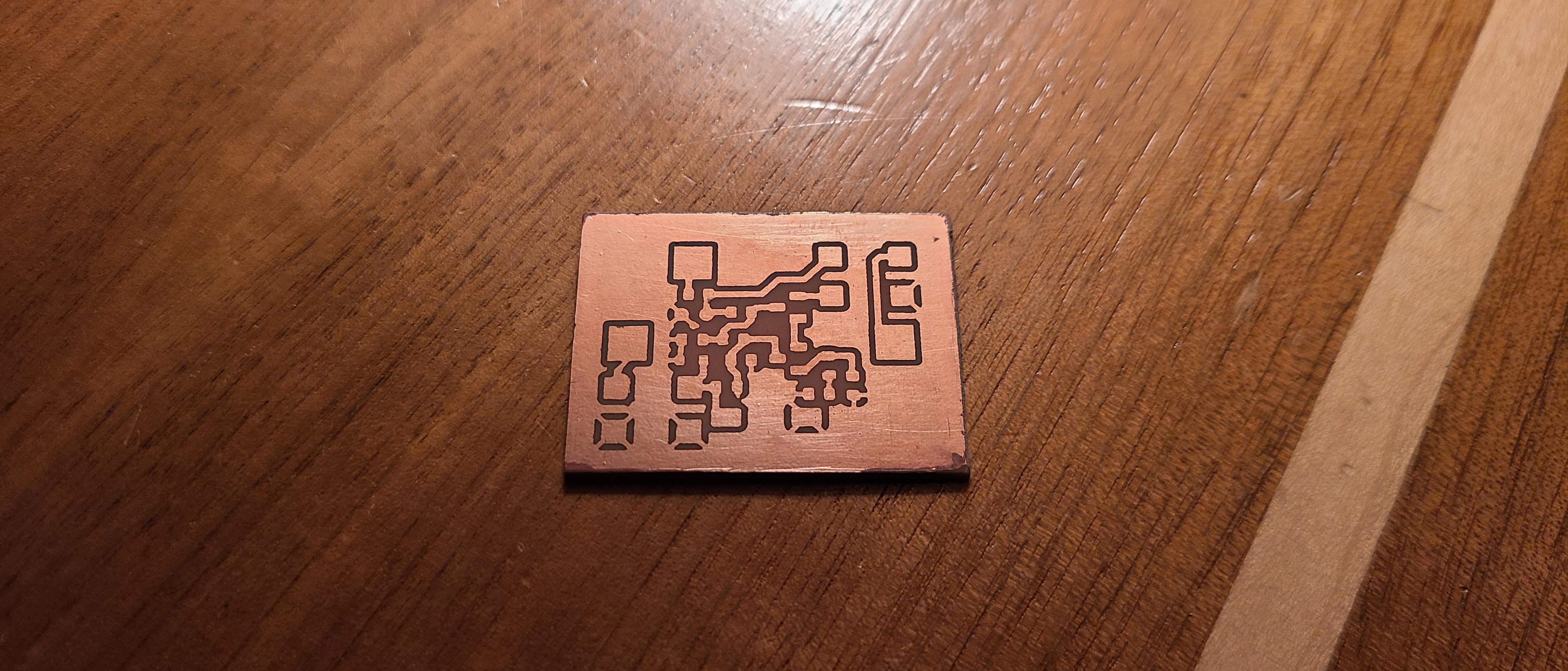
Building the PCB
Being that I have begun making my own boards at home, I decided to etch this design into some copper clad board. I started by designing the PCB layout in KiCAD, then printed it out on some gloss paper. After printing, I transfered the toner onto the copper clad board. I then etched the board in ferric chloride etchant.
After etching, I soldered the components to the board. I opted to use 1/8 W axial through hole resistors as I have been running low on chip resistors. The transformers were hand wound using 28 AWG wire around a 43-mix fair-rite toroid. I used X7R chip capacitors and a through hole ceramic decoupling capacitor on the power supply. For the input bandpass filter, I included a trimmer capacitor to tune the circuit.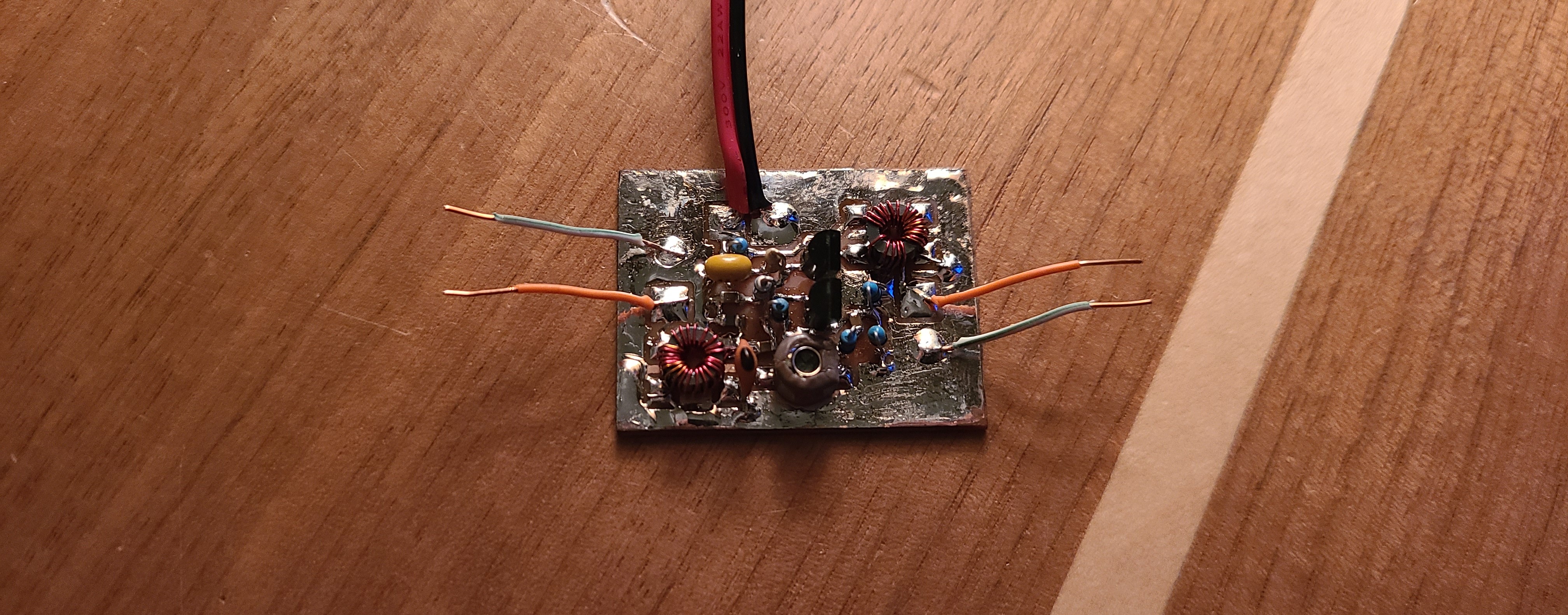
Testing
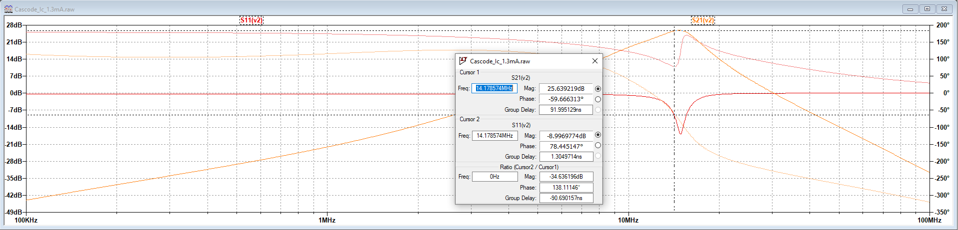
I used my NanoVNA and TinySA to test the circuit. I couldn't properly test the output impedance of the circuit due to the attenuator I added at the second port of my VNA.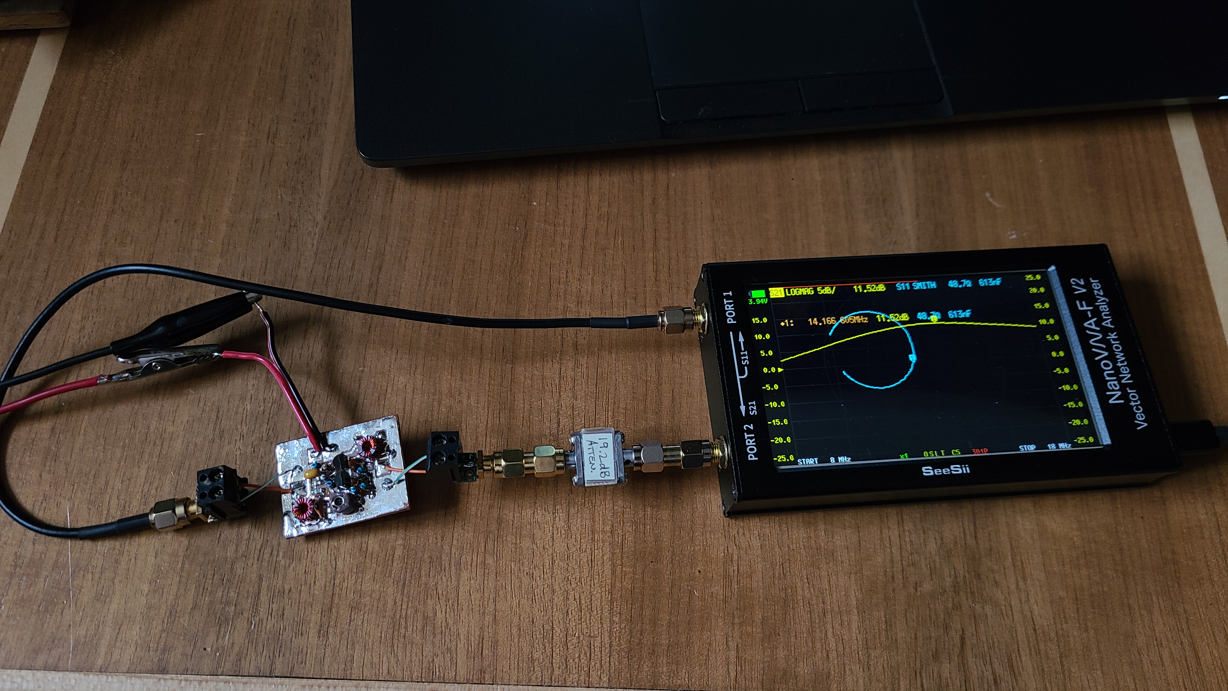
The results of the NanoVNA measurement was fairly decent. My input impedance was close to 50 ohms and I achieved a gain of 11.5 dB.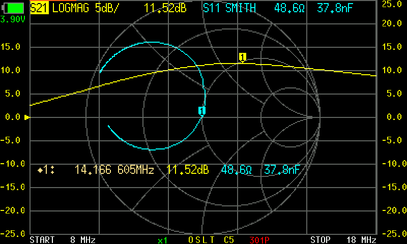
These results are definitely far from the simulation, but it was still decent enough for my application. I was more happy that the input impedance was matched.
I also tested the output of the amplifier on the TinySA. Using the NanoVNA as a CW generator, I used the TinySA to measure the noise floor.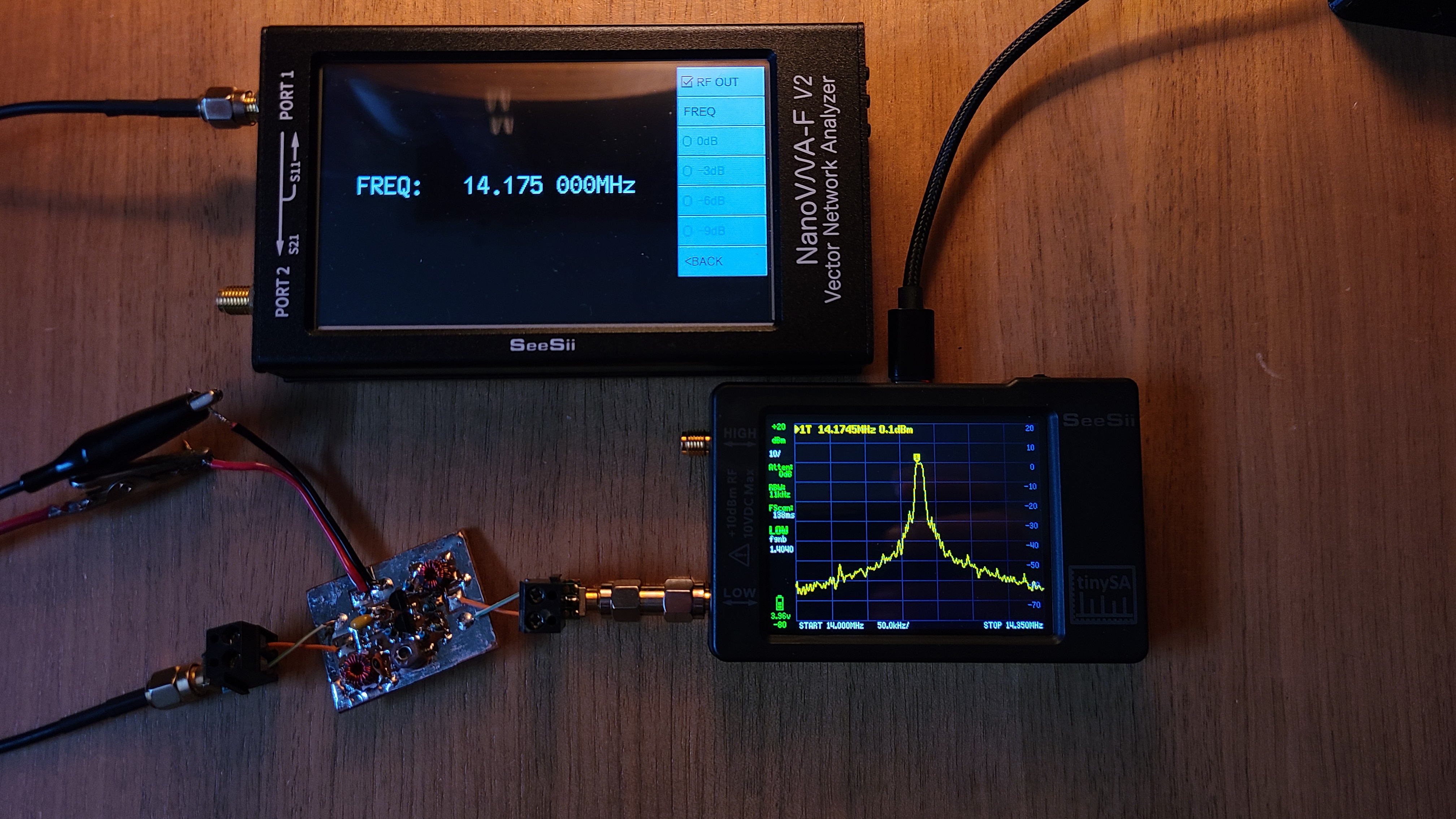
Results of the CW test shows the noise floor being amplified by the same amount as the signal.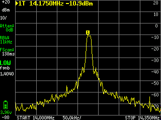
I am new to spectrum analyzer measurements for noise figure, so I am actively researching how I can measure the noise figure of my amplifiers using this tool. In the future, I also plan to use my function generator to generate two non-harmonically similar signals to practice testing linearity.
Remarks
Modified Spice Simulation
Unhappy with the output impedance results, I tinkered with the output transformer and found a ratio of 16:1 was optimal for achieving the desired 50 ohm output impedance. This also increased the gain by 5 dB (whether this works in reality is a different story).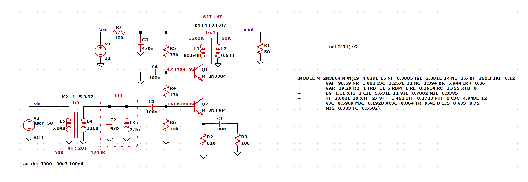
In future designs I will apply what I have learned here to ensure I achieve better results.
This amplifier seems to work well, although I am not fully satisfied with the output impedance situation. My goal with this amplifier was to ensure the gain wasn't too high and to match this input impedance, so I achieved what I intended on achieving. Now that I have learned more, I get to improve the next design that much more.
For now I will aim my focus towards making a proper test bench to provide a proper ground plane for all my radio building blocks. I am also looking into improving my antenna outside my house. Stay tuned in if that interest you!