Since my last attempt at a variable gain intermediate frequency (IF) amplifier, I took a pause on my HF superheterodyne project. Recently I decided to tackle the variable gain amplifier (VGA) design.
My previous design had many flaws which the new design I came up with solved.
The Topology
After looking into all sorts of topologies that only employ the use of bipolar transistors, I found what I like to consider a current steering cascode variable gain amplifier. This amplifier takes a standard cascode topology, and adds another BJT (Q3 in the figure below) to "bypass" the common-base transistor (Q8) in the cascode. By varying the current into the base of this new BJT such that the base voltage is around the bias voltage of the cascodes common-base transistor, the current is steered between the main branch or the newly added transistor.
This allows me to control the amount of current the common-base section is able to utilize which in turn allows me to control the transconductance of Q8 ($g_{m8}$), while maintaining the original operating point of the input transistor Q1.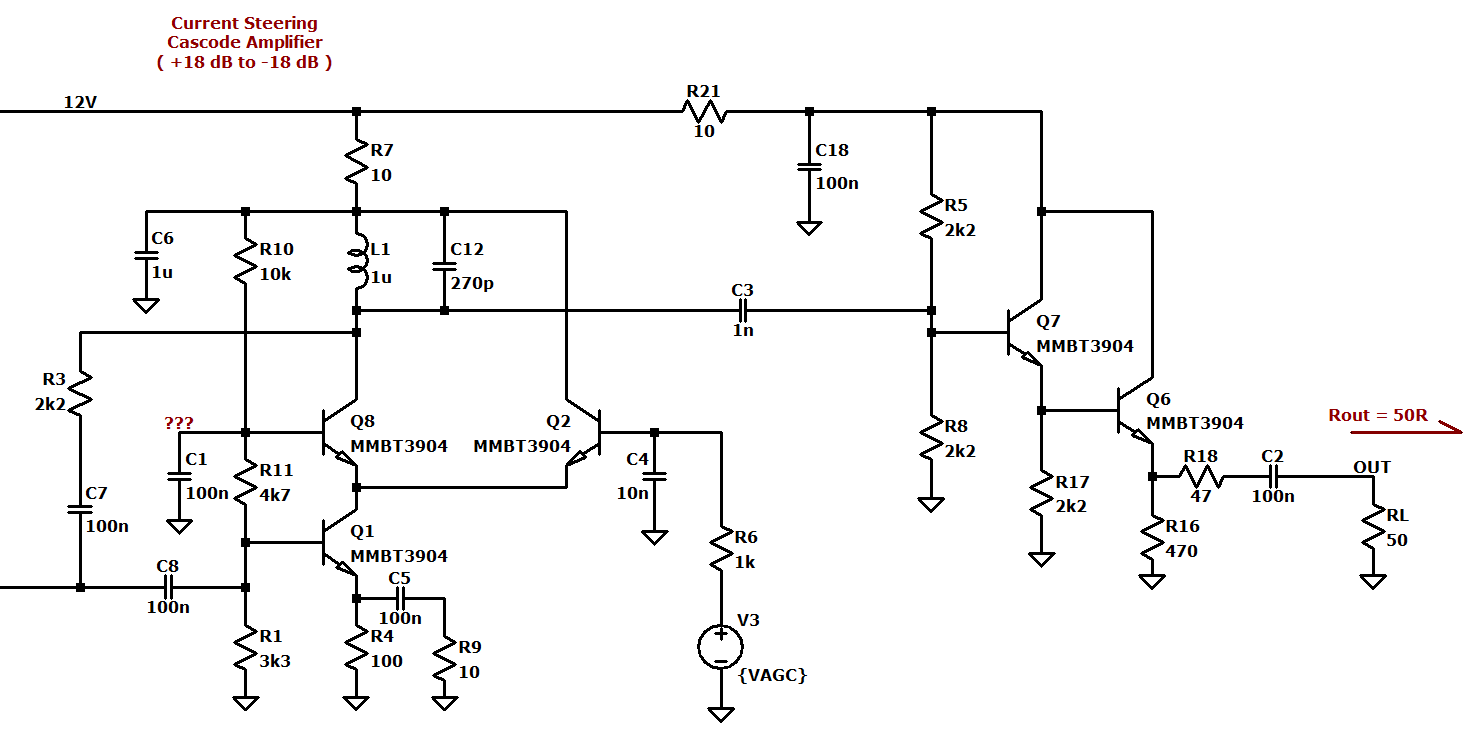
This also means that as the gain is reduced, the miller effect may be less suppressed as $g_{m8}$ gets further from $g_{m1}$. With an IF of 9.830 MHz however, this shouldn't be an issue for the MMBT3904's that I am using.
Simulations
To fully simulate this circuit, I added a W7ZOI termination insensitive amplifier as a first stage to provide constant input impedance and 20 dB of gain. The Current steering cascode is able to not only provide gain, but also attenuation, so by adding 20dB of gain prior, I can get a gain between 0 and 40 dB.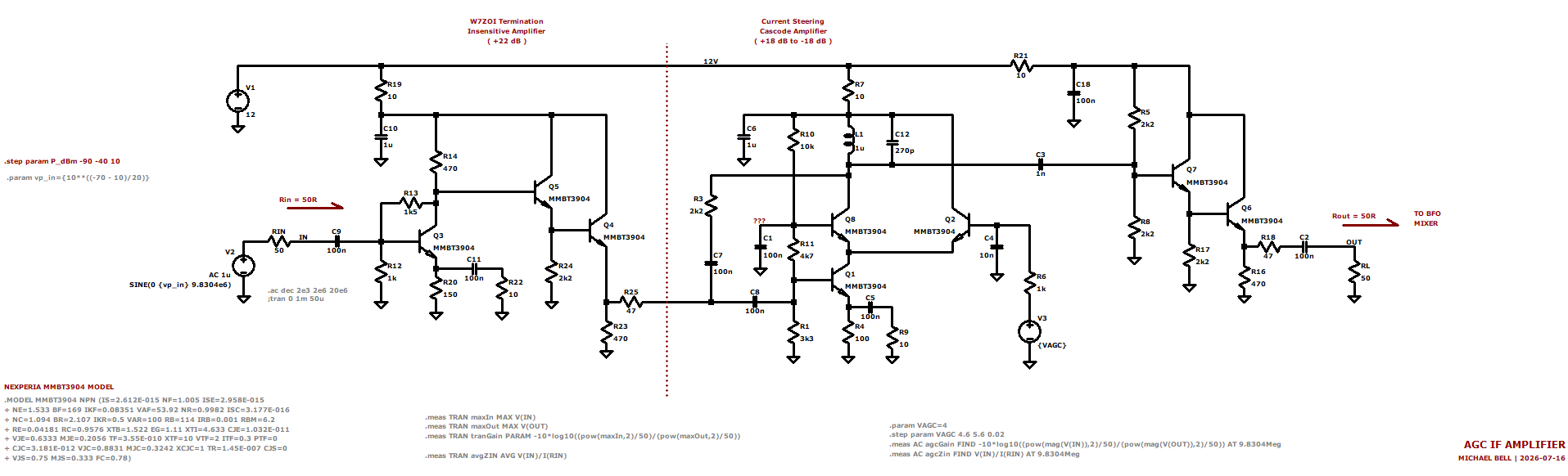
The resulting AC analysis at each AGC voltage shows a good response, with the amplifiers gain sitting at roughly 42 dB.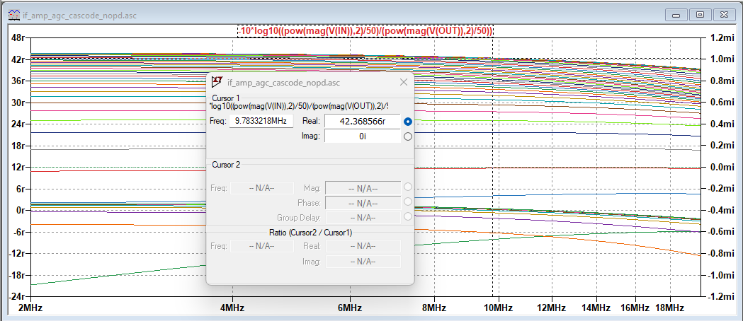
Next I took the stepped data and measured the gain at 9.830 MHz for each step of the AGC voltage. The vertical axis represents amplifier gain in dB. The horizontal axis represents the AGC voltage (don't be fooled! LTspice is labelling it as Hz, but it is voltage).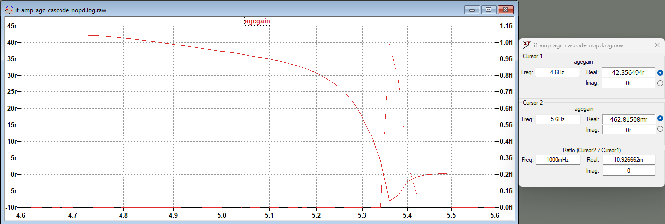
Constructing the PCB
After successful simulations, I etched a PCB following the schematic and soldered together all the necessary components.
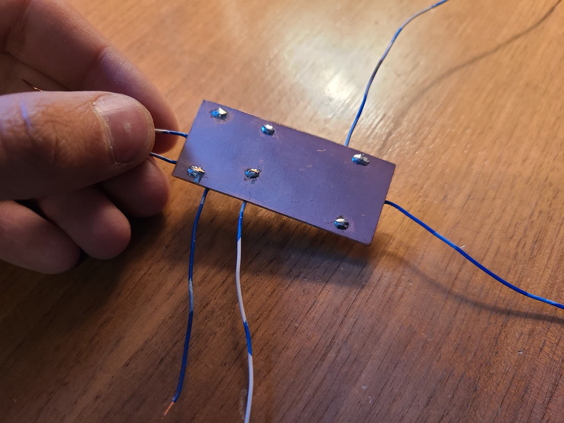
Unlike my past designs, I have begun using double sided copper clad board to incorporate a good ground plane. I chose to do this is because my designs have been increasing in gain (30 - 40 dB). With a ground plane I can create short low-conductivity grounds for bypass capacitors as well as ensure amplifier stability.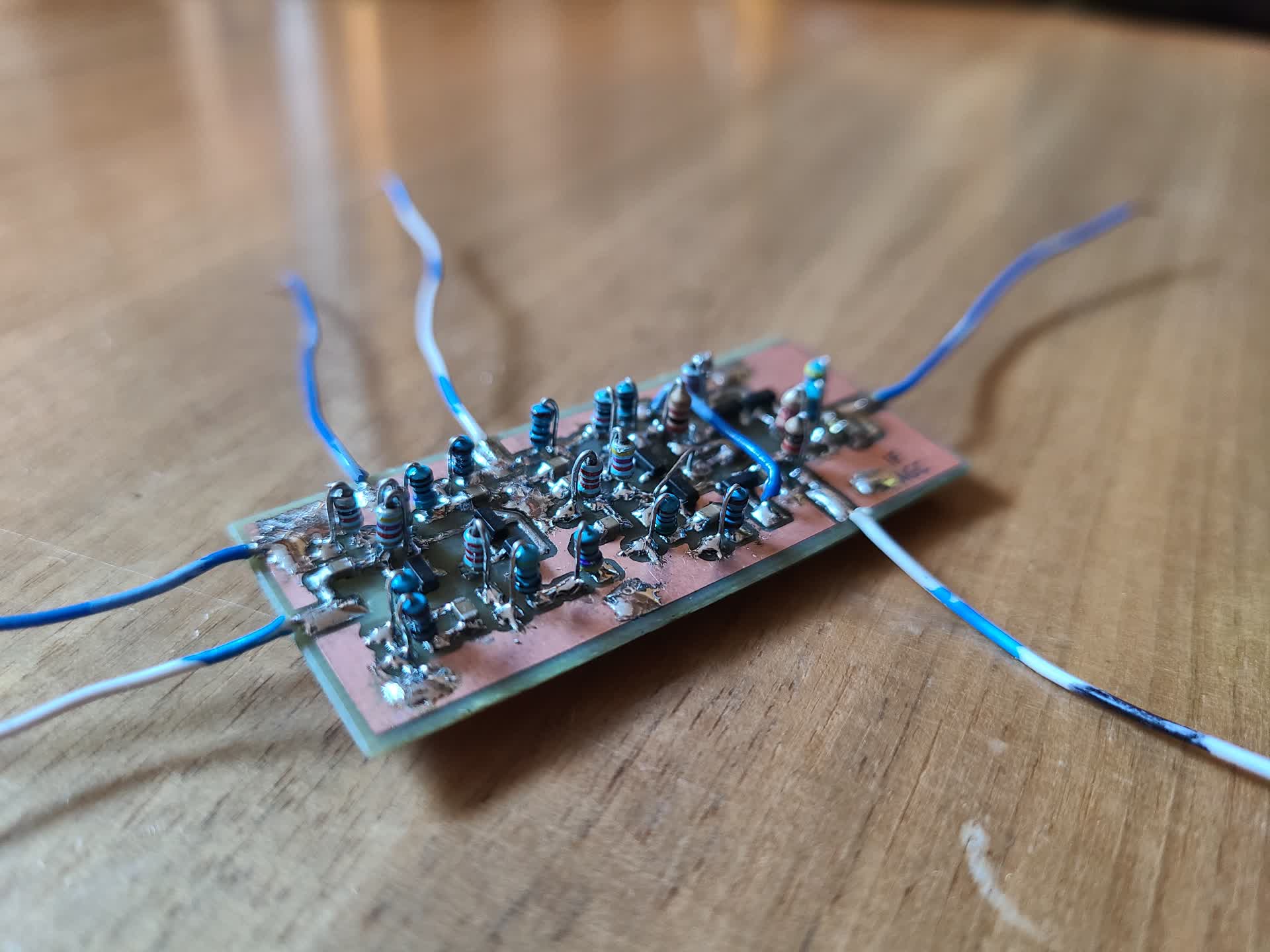
Bench Tests
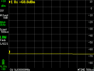
To test the VGA I used a function generator set to 9.830 MHz at -10 dBm, then routed that through my attenuator box with 50 dB of attenuation. Measuring the input signal using my TinySA spectrum analyzer set to zero-span showed -68.8 dBm.
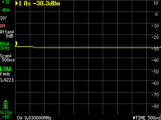
After I then connected the amplifier with its AGC voltage node grounded to achieve its maximum gain. This resulted in a gain of -30.3 dBm. With these two measurements I determined the amplifiers gain to be 38.5 dB, which doesn't fall very far from the simulated 42 dB of gain.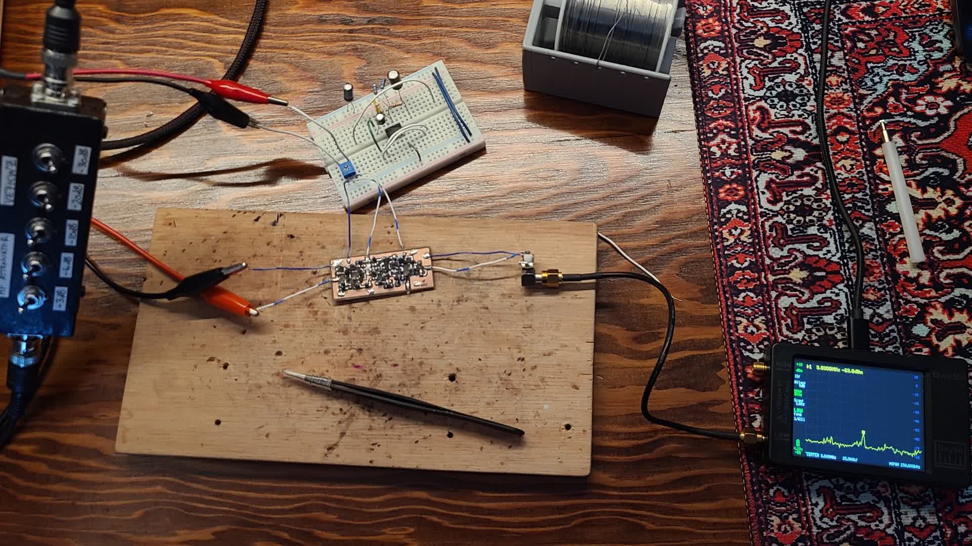
Lastly, controlling the AGC voltage using a 5k ohm potentiometer connected between 12V and ground I demonstrate the variable gain this amplifier can achieve. Because the gain varies between 4.7 and 5.4 volts, the gain changes fast as I turn the potentiometer.
I have been making aditional experiments with an AGC circuit, which I show the results of half way into the video where I connected it in.