After designing the tuned IF amplifier, I wanted a second IF amplifier that handled most of the receiver's gain. This ended up being more of a learning experience than I anticipated.
For the majority of this superheterodyne receiver project, my amplifiers have all been in the cascode configuration. I did this because it mitigates the Miller effect, which the 2N3904 and MMBT3904 transistors are subject to at high frequencies.
In this post, I walk through two cascode amplifiers I built. While one was functional, the process really taught me the importance of checking the non-linear transient behaviour of my circuits.
Don't use this Amplifier Design!
The designs in this page are experimental and didn't work properly. I explain in the post.
Single Stage Amplifier
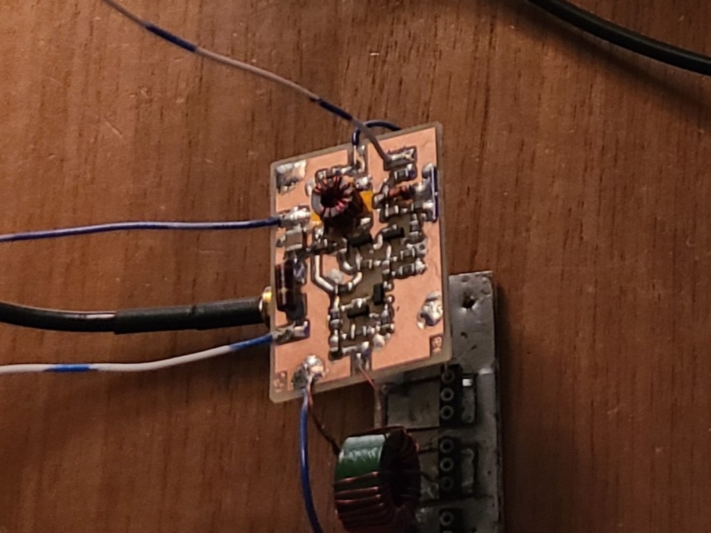
The first amplifier I made was a single cascode stage with two common collector buffer stages at the input.
Using a 1N4148 diode to control current through the emitter's AC degeneration loop, I could control the gain through negative feedback. The issue with this was the input impedance variations.
The idea I implemented was to use common collector stages to keep the input impedance at a constant 1 kΩ isolating the cascodes varying input impedance from the input of the amplifier.
The AC simulation for this amplifier proved the idea worked for implementing electronic gain control. The input impedance was very stable at 1 kΩ, and the gain varied between around 9 dB and 20 dB proportionally to a gain control voltage.
Construction
I built the amplifier using a home-etched board.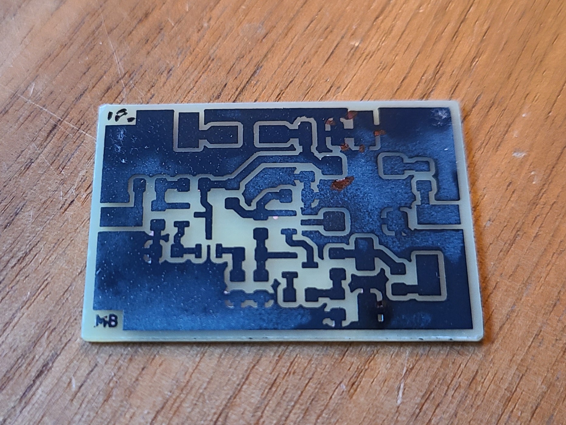
Testing
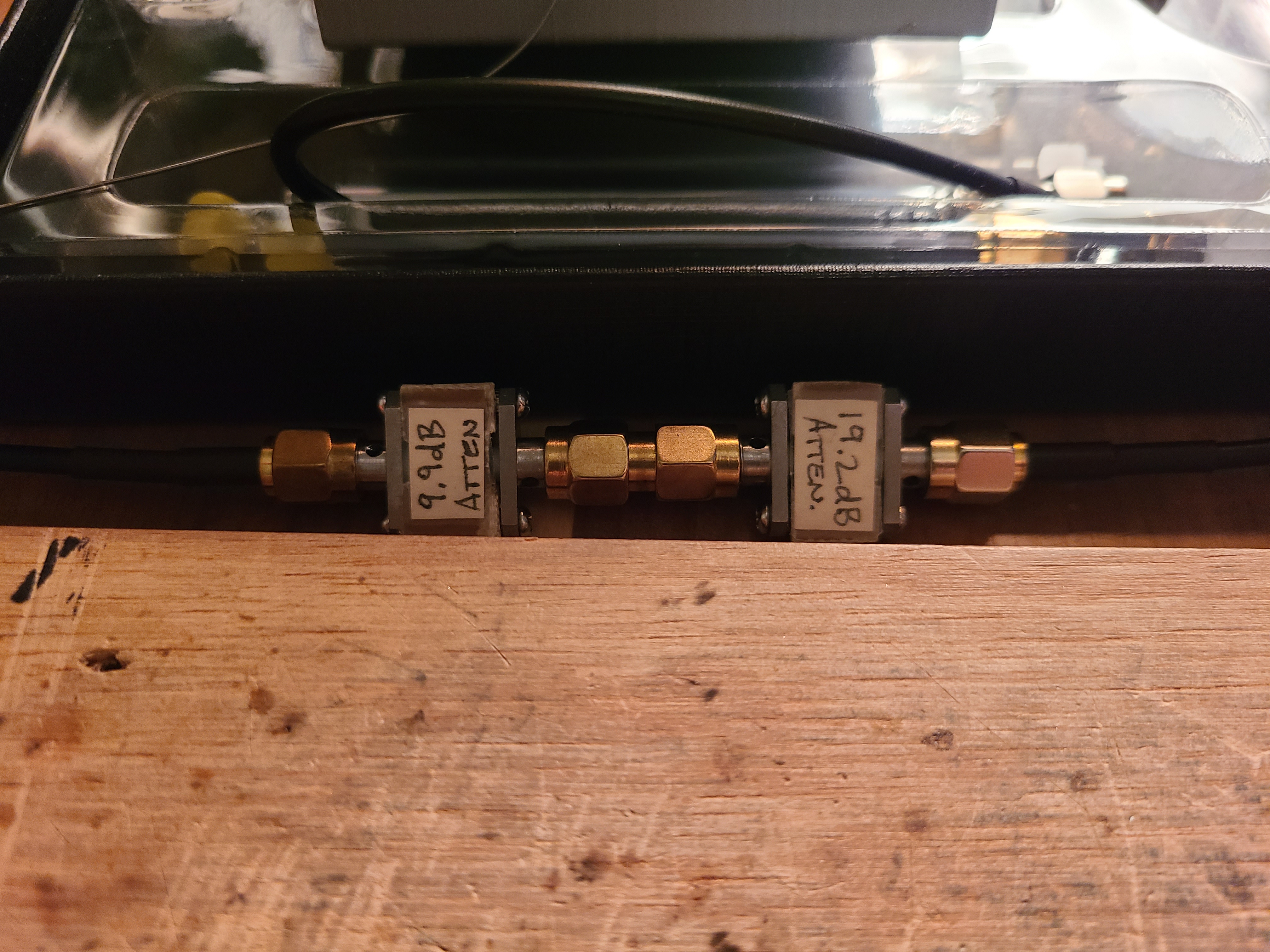
Using my test jig and a 50 Ω to 1 kΩ transformer at the input, I measured the input gain using my TinySA.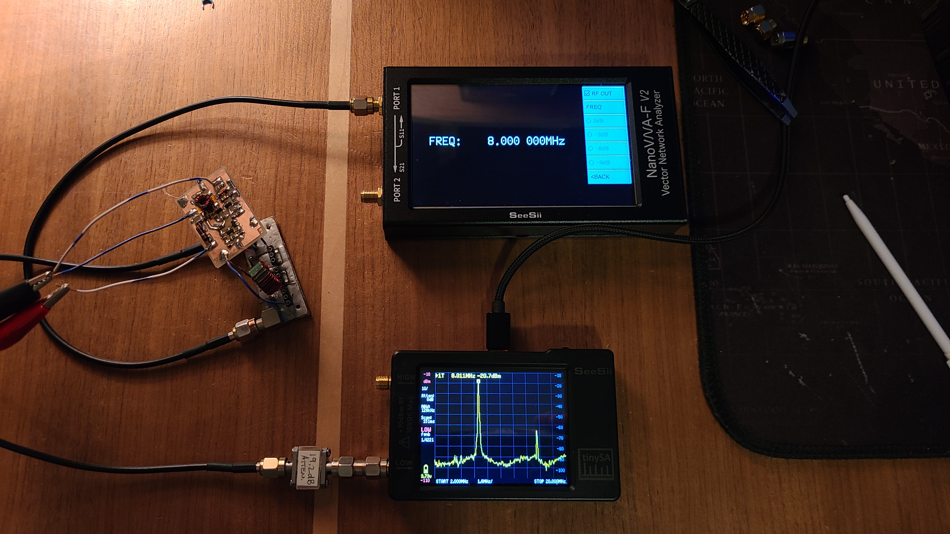
Looking back on the test setup, the NanoVNA output power in RF generator mode is roughly -9 dBm. Using additional attenuation on the NanoVNA's output would have been more accurate as to the power levels the amplifier may see.
The impedance was measured to be very consistent at minimum and maximum gain.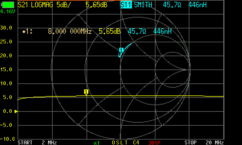
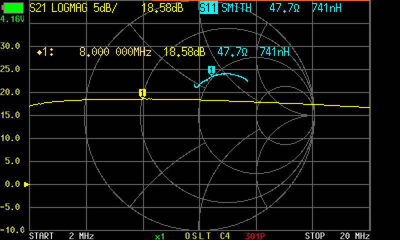
The gain variation was not as wide as shown in the LTspice simulation, but it was very close. This gave me confidence in the design.
For the TinySA measurements, I should note the NanoVNA uses a square wave output. The second peak shown at 16 Mhz is the first harmonic of the 8 MHz fundamental.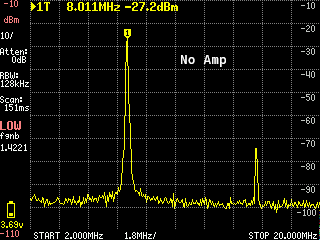
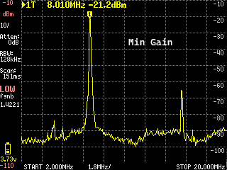
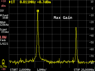
Overall, the amplifier produced a minimum gain of 6 dB, and a maximum gain of 18.5 dB.
Two Stage Amplifier (The eye opener)
Unfortunately at the time of writing this post, I have overwritten the LTspice simulation for the second IF amplifier design. The schematic is a simple expansion on the previous design, but with an additional common collector buffer and cascode gain stage.
In LTspice, an AC analysis showed a gain of 20 - 56 dB over a control voltage of 0.2 - 0.8 volts.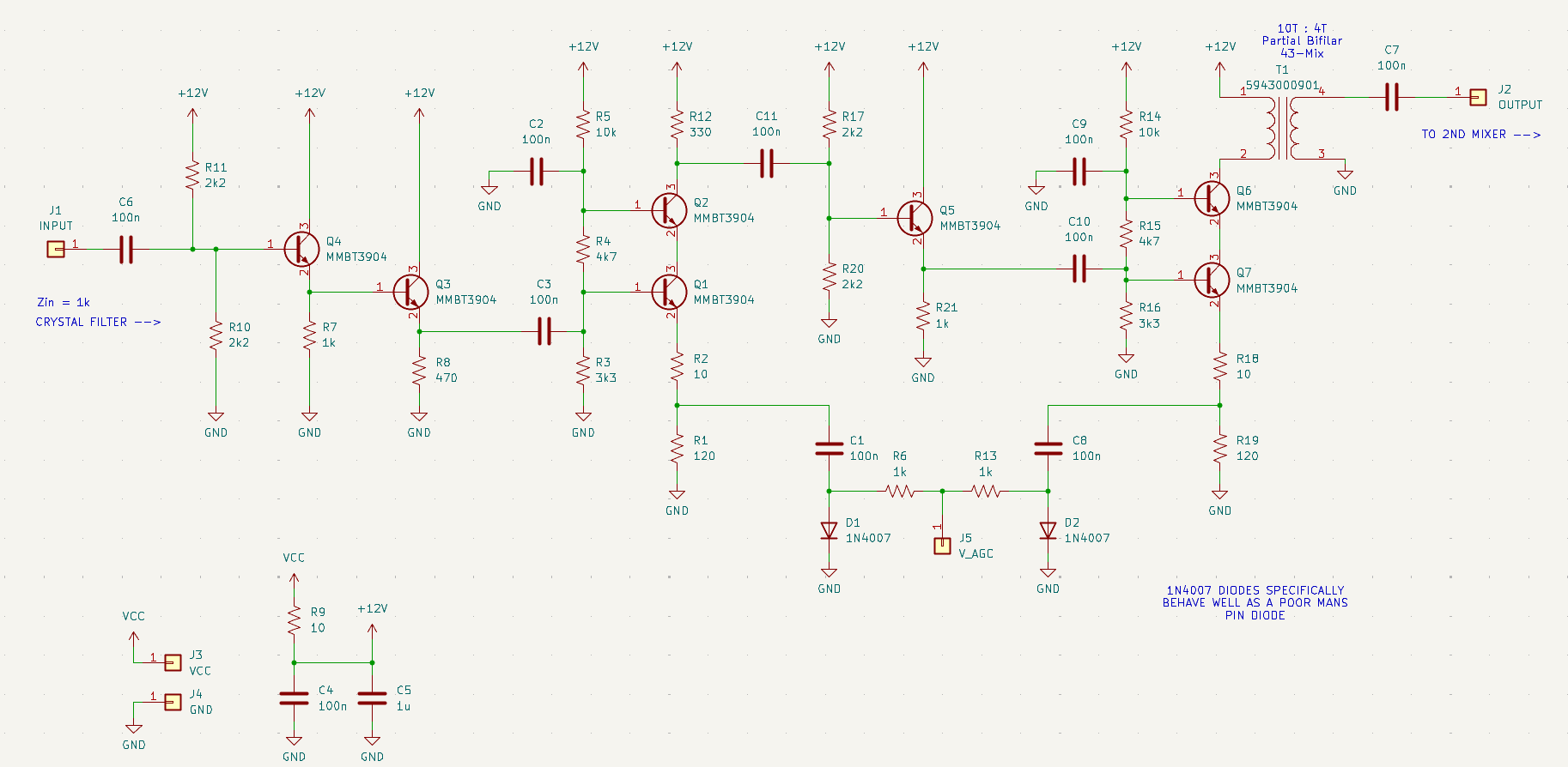
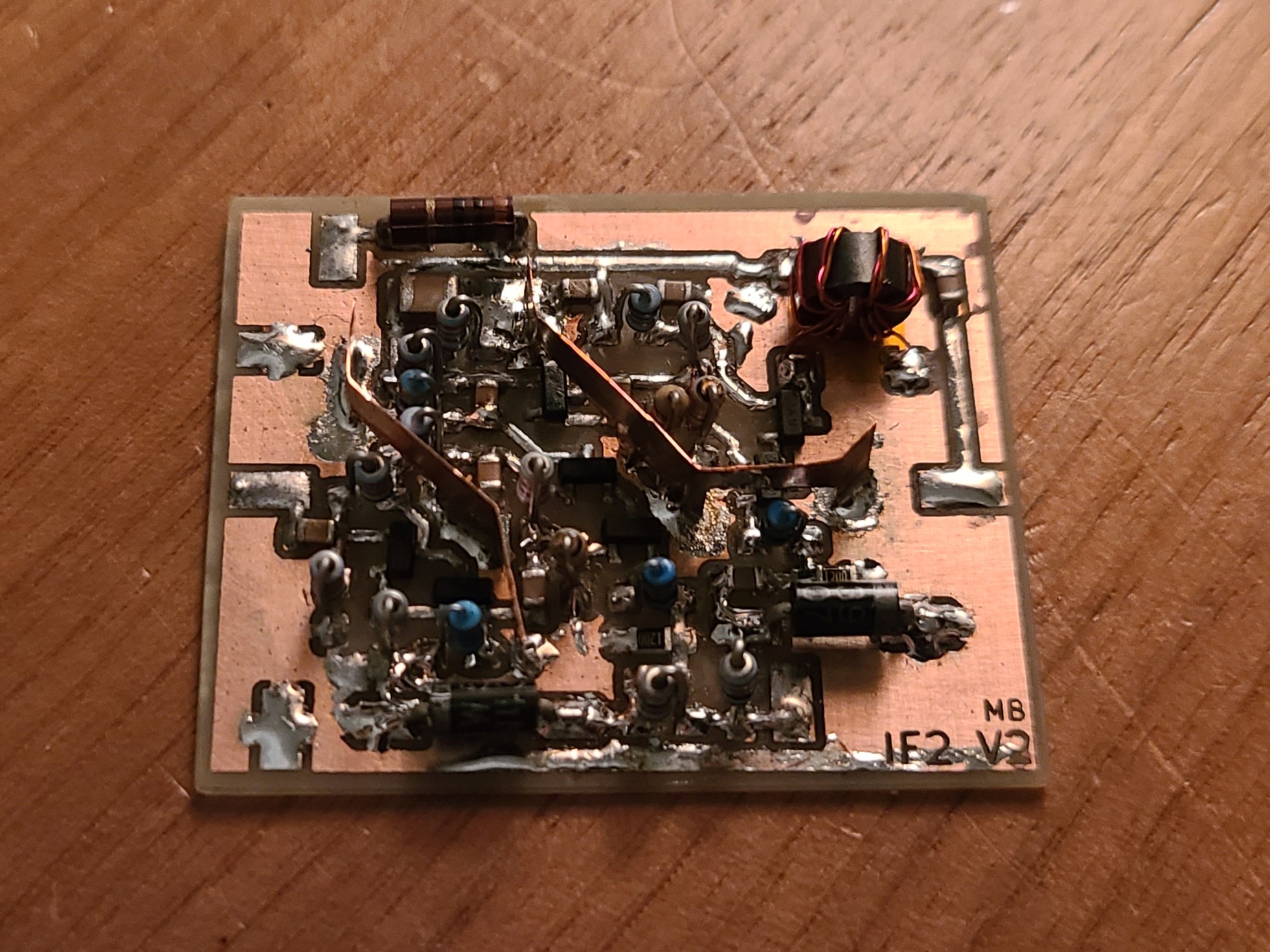
Construction
The amplifier was fun to build because it looked complex and felt like a behemoth.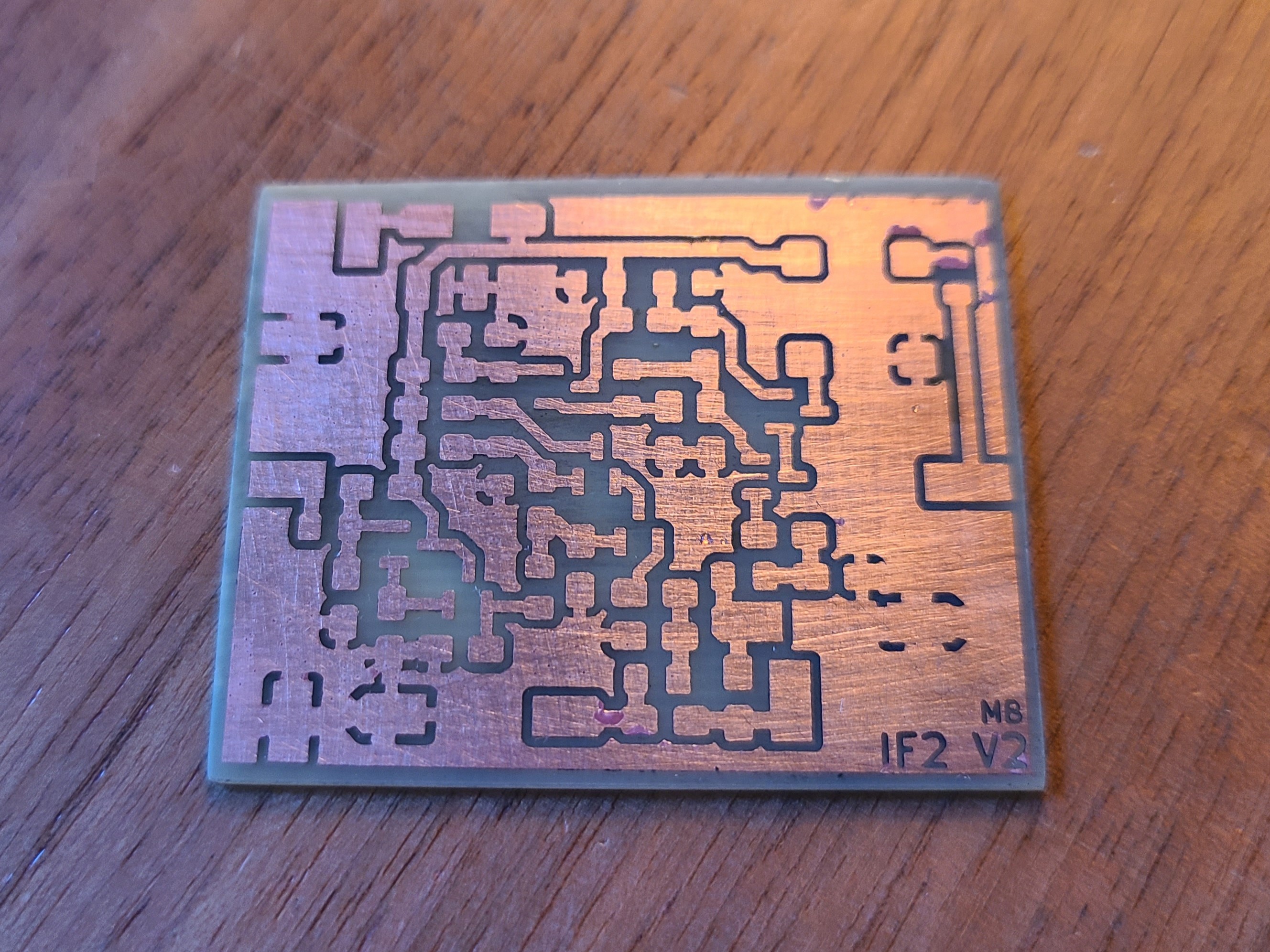
Testing
When testing this amplifier, I was hoping to see a crazy gain of 50 dB and jump in joy. That did not happen. This is where I learned a hard lesson in amplifier stability.
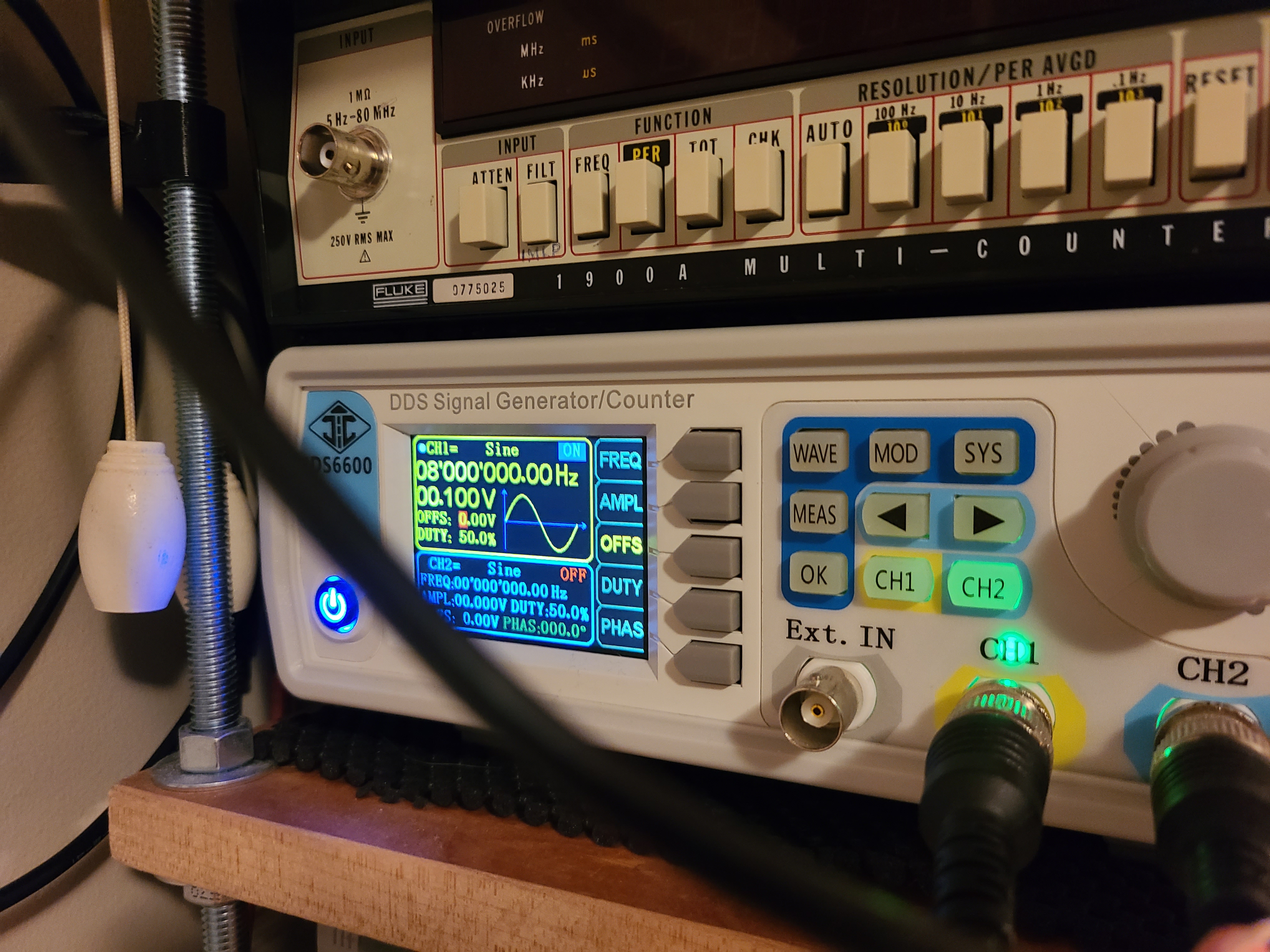
To test the amplifier, I used my function generator as it can output a sinewave (no harmonic content). With the function generator outputting about -20 dBm, I added about 30 dB of attenuation on top of it. This was in preparation for the (expected) 50 dB of gain.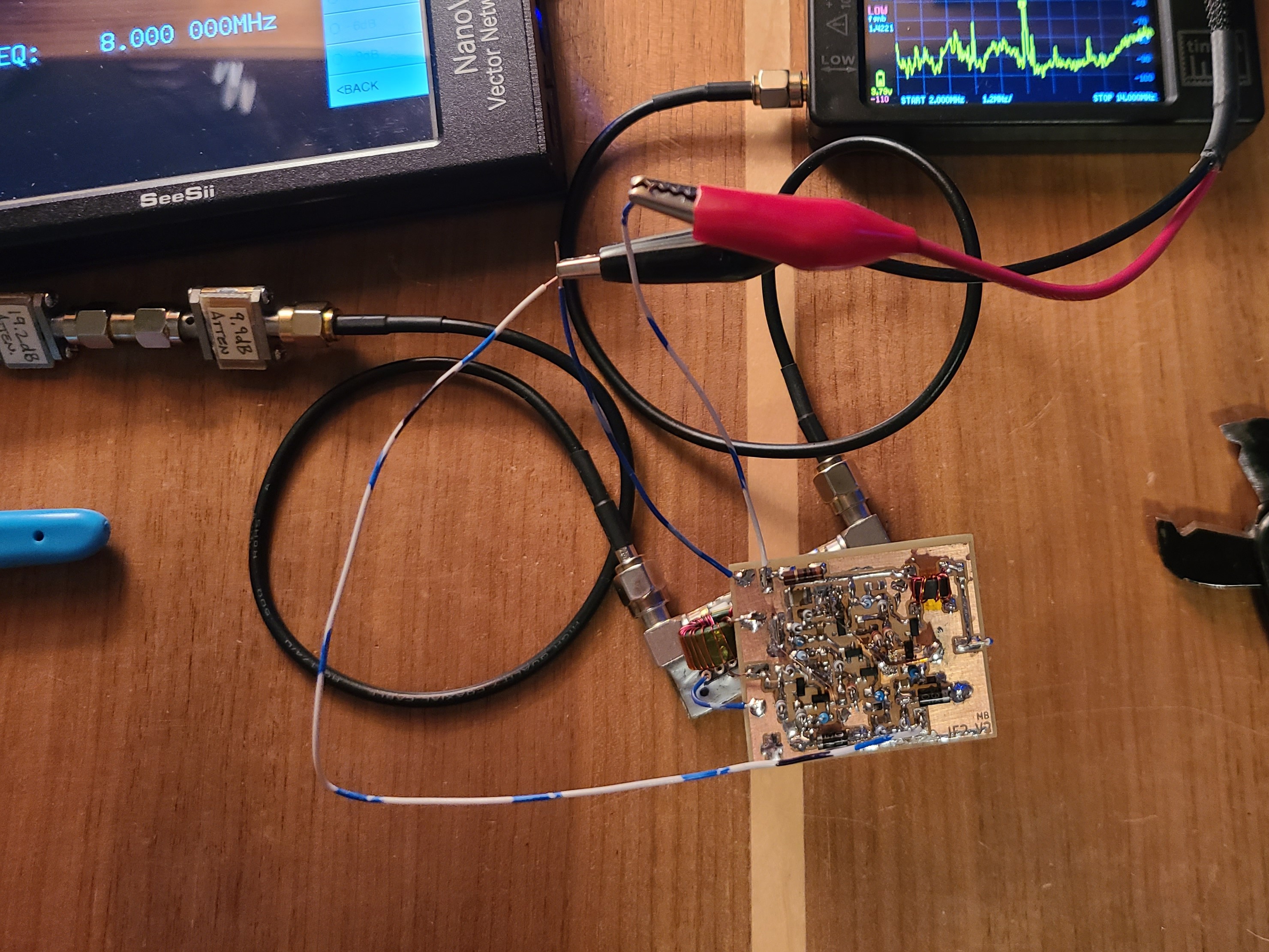
Connecting everything together, I measured the results on my TinySA.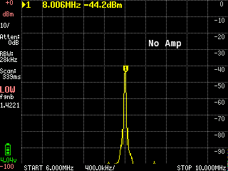
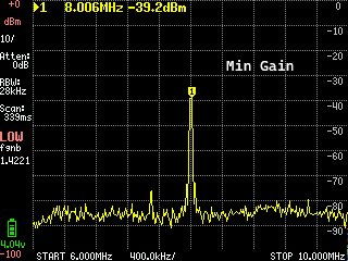
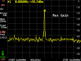
The results were, 5 dB gain minimum, 23.5 dB gain maximum. This was way off from my expected gain.
I kept testing late into the night, using my oscilloscope to see what the output waveform looked like. Unfortunately I didn't capture any pictures.
When viewing the waveform, I saw modulation and distortion from the amplifier.
I ran a transient simulation in LTspice and realized how poorly designed this amplifier truly was.
Remarks
From here on, I plan to look closer into a designs transient response for linearity and stability.
Lessons were learned, and experience was gained. The main theme of engineering is failure, but that's what makes success feel so great.