In the autumn of 2023, I volunteered to create and present a printed circuit board (PCB) design workshop for the University of British Columbia Okanagan's (UBCO) IEEE McNaughton Learning Resource Center's (MLRC) Hackerspace (whew that was a mouthfull!).
Now, I did this the previous year, and while it did have an attendance somewhere in the range of 40 students, it was fairly new and also my first time hosting an in-person event like that.
This newly revised PCB design workshop was simply a polished version of the 2022 EWorkshop.
As for the EDA, I chose to use KiCAD as it is a free and open source EDA with a reputation as the go-to hobby and startup PCB design software. Additionally, KiCAD is similar enough to industry standard software such as Altium Designer, that it should help students that are unfamiliar with PCB design adapt to various other EDAs.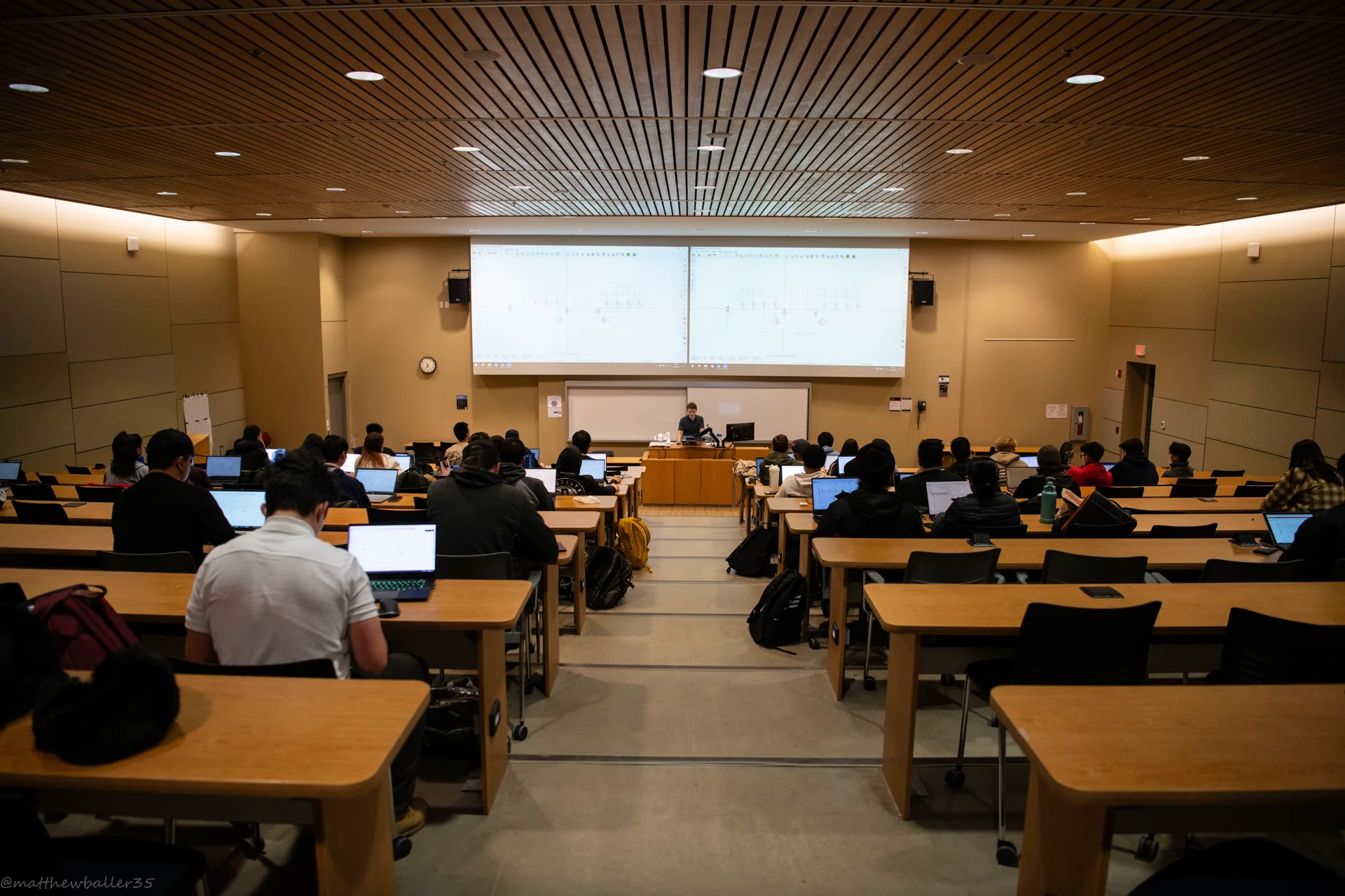
EWorkshop Event Presentation and Structure
The workshop was built around the circuit and PCB design, but generally speaking, it covers the following:
- Introduction to the KiCAD software - A brief run through of the project creation process.
- Drawing schematics, searching for and placing symbols, and editing symbol preferences/data and associated footprint.
- Sourcing parts from sites like DigiKey and Mouser.
- Generating a bill of materials (BOM)
- Configuring the PCB editor, setting DRC tolerances, importing footprints, and PCB layout.
- Running design rule checks on the final PCB design and exporting gerber (manufacture) files.
- Ordering PCB's from sites like OSH Park, PCBway, and JLCPCB.
On later dates, students could also come to the hackerspace to learn how to solder the PCBs.
Documents
Most of the work went into generating documents such as the presentation, and supplimental docs. I made the presentation and presenter notes to be simple yet informative.
The presentation introduced students into what a printed circuit board consists of, what a stackup is, and some of the history behind PCB's.
The supplimental documents took more time, as the information needed to be gathered. The "best practices" documents contain what I believe to be best practices, but that is always subject to change and there are no hard rules. At the end of the day, the goal is to create clean and consistent schematics and PCBs.
I have forked the information from the schematic design best practice and PCB design best practice to my notes section of my site which has my updated and most recent personal best practices that I employ.
The Circuit and PCB
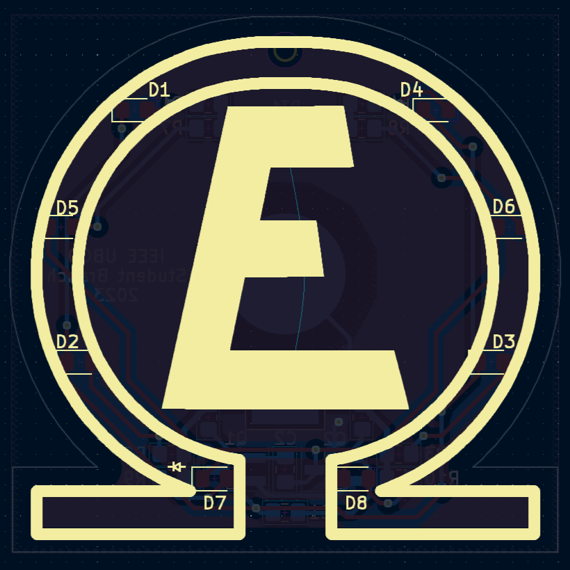
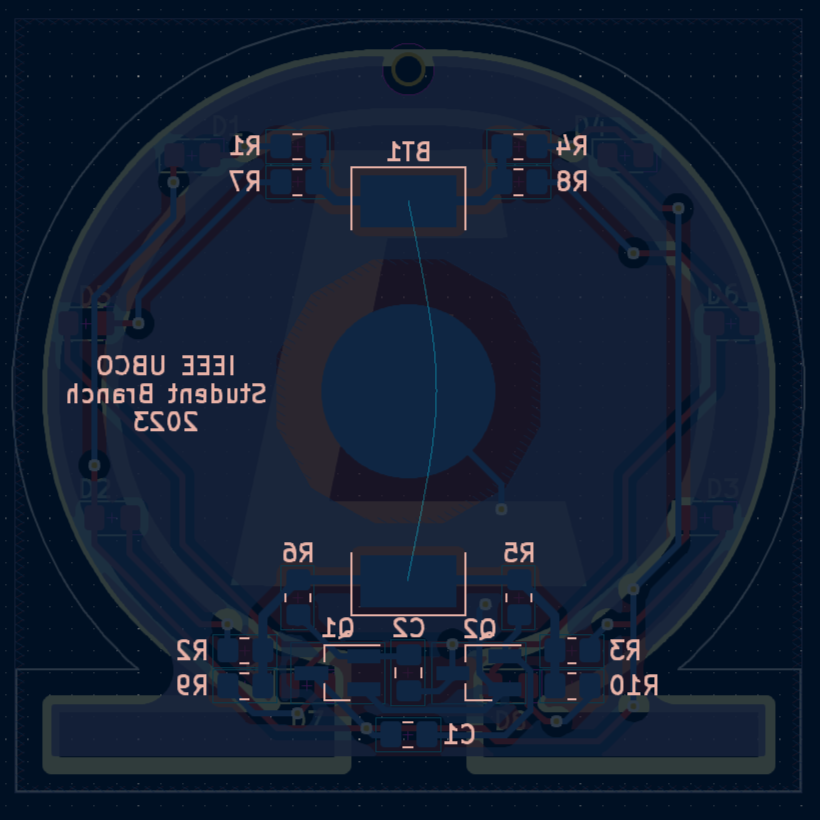
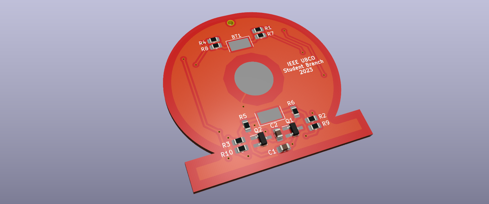
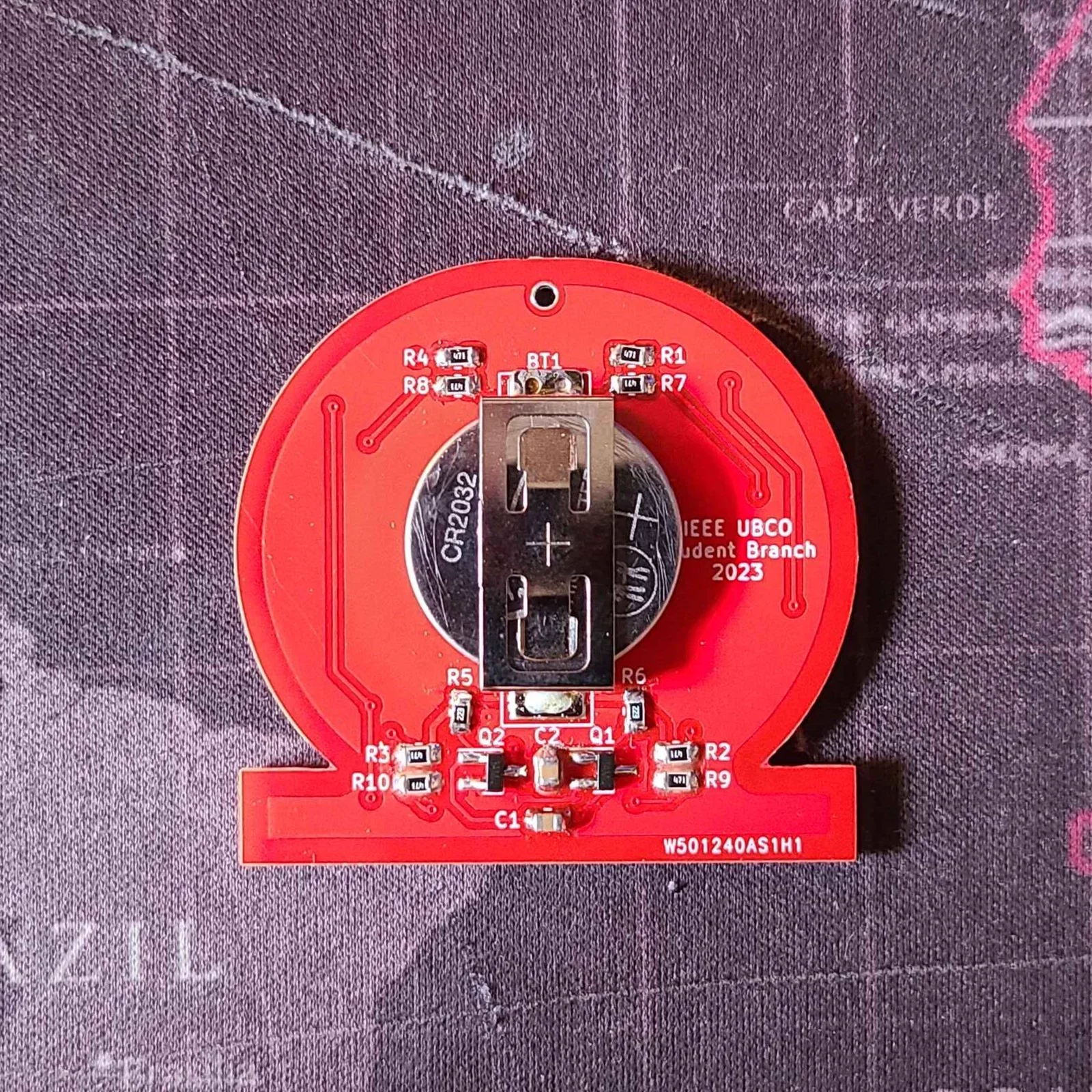
To get started on organizing the workshop, I needed a circuit to design. The president of the UBCO IEEE MLRC Hackerspace showed me a decade-old PCB from the previous student that ran the space, and using that as a reference, I came up with the idea of a badge with blinking LED's. Simple, yet interesting.
Using a basic astable oscillator design using two NPN BJT's I threw together an 8 LED blinking circuit. Using the Falstad Circuit Simulator I put together a simple animation to demonstrate the circuits operation.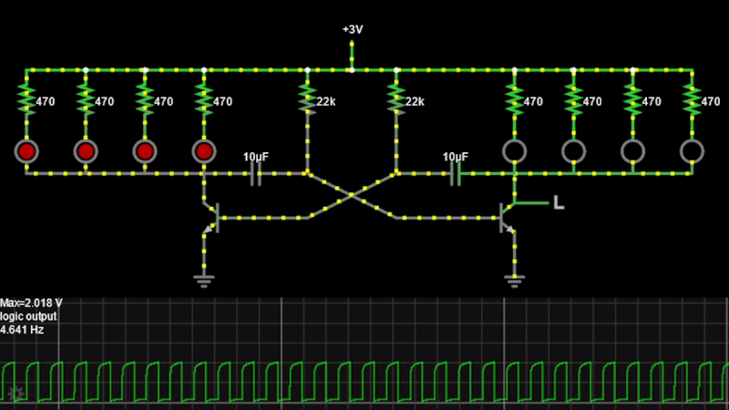
After, I proceeded to draw the schematic in KiCAD. At the same time, I sourced the parts as needed and included their information (datasheet, footprint, etc.) within each schematic symbols data.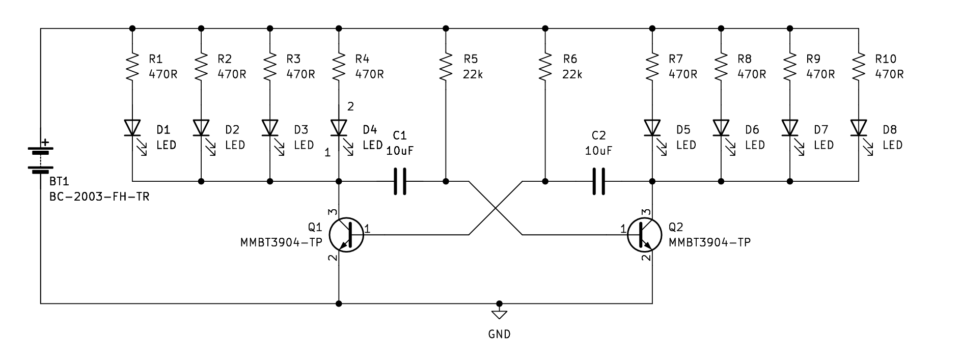
PCB Layout
Once the schematic and parts were picked out, the PCB was laid out.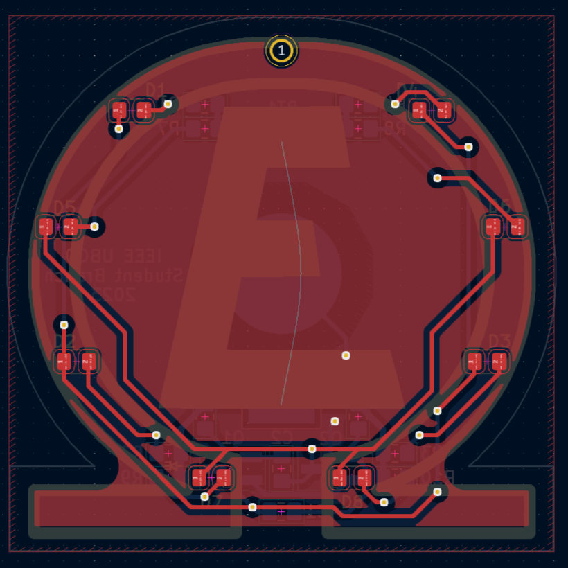
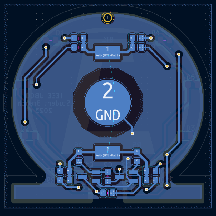
The complete PCB will be ordered to have a red solder mask.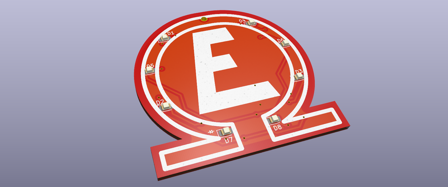
Workshop Event
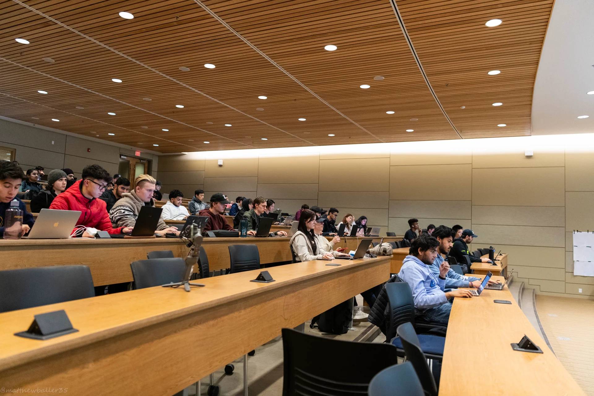
The workshop was a success, with an attendance of around 55-60 students. I was able to pace the workshop in such a way that there was plenty of time for questions, help, and tangents.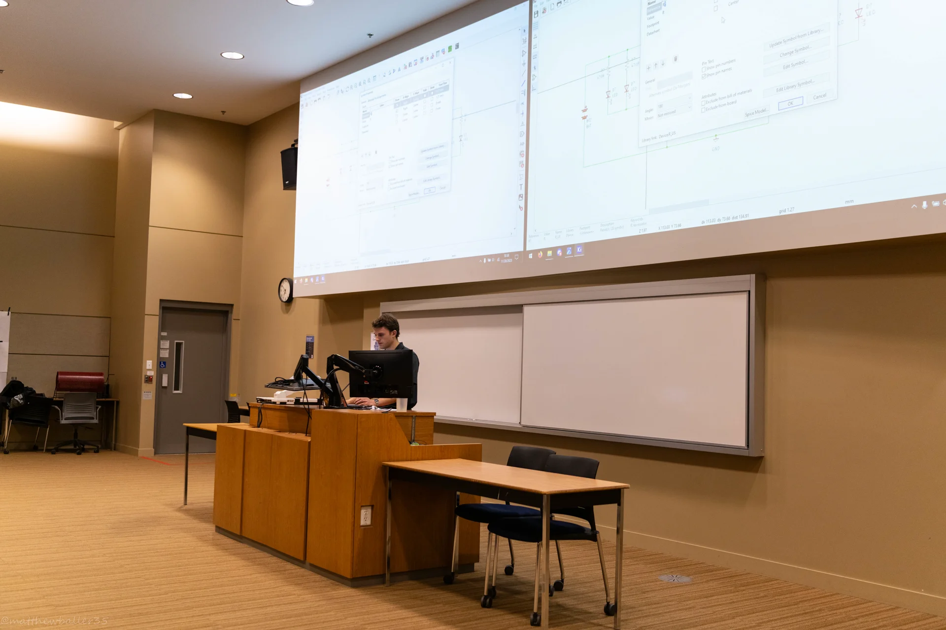
The final result of the PCB workshop was a lovely badge that students could wear, or tie a string to and hang. It could even be used as a Christmas tree ornament!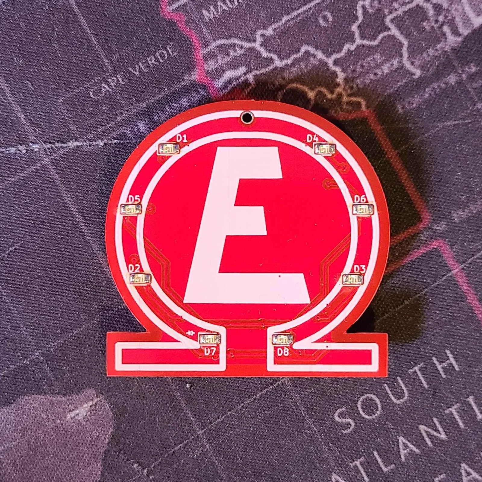
![]()