During my ENGR 458 Power Electronics course, I participated in a mini project where my group built a physical DC-DC boost converter from scratch on a breadboard. We designed the system to convert a +12 V input into a +48 V output, capable of delivering 10 W of power to a 233 ohm load. Operating at a switching frequency of 100 kHz, the converter was strictly optimized to keep the output voltage ripple under 1%.
DC-DC SMPS Design & Test
The circuit design follows a standard boost converter topology utilizing specific power components. An NXP PHP23NQ11T N-channel power MOSFET serves as the primary switch, driven by a MICREL MIC4420 low side driver capable of delivering a 6 A peak output current. For rectification, an SMC 12TQ100 Schottky diode was selected due to its 15 A forward current capability.
The passive components are quite simple. The capacitor used was a 560 uF Aluminum Electrolytic capacitor rated for 80 V. The inductor was hand-wound on a TDK B64290L0058X830 ferrite toroid. The target inductance was between 35 mH and 54 mH. Given the toroid has an AL value of 4.36 uH (+/- 25%) we calculated the number of turns to be around 100 turns.
The passive component selection focused on power handling and stability. Output filtering is provided by an 80 V rated, 560 μF aluminum electrolytic capacitor. The inductor was custom fabricated by hand winding 28 AWG insulated wire onto a TDK B64290L0058X830 ferrite toroid. To meet the target inductance range of 35 mH to 54 mH with the core's $A_L$ value of 4.36 μH (± 25%), approximately 100 turns were applied. The final inductance value was verified in the lab using an LC meter. Additionally, a 5 W, 1 Ω resistor was placed in series before the inductor to safely facilitate current measurements.
Using 28 AWG insulated wire we wound the inductor and tested the inductance using an LC-meter in the lab.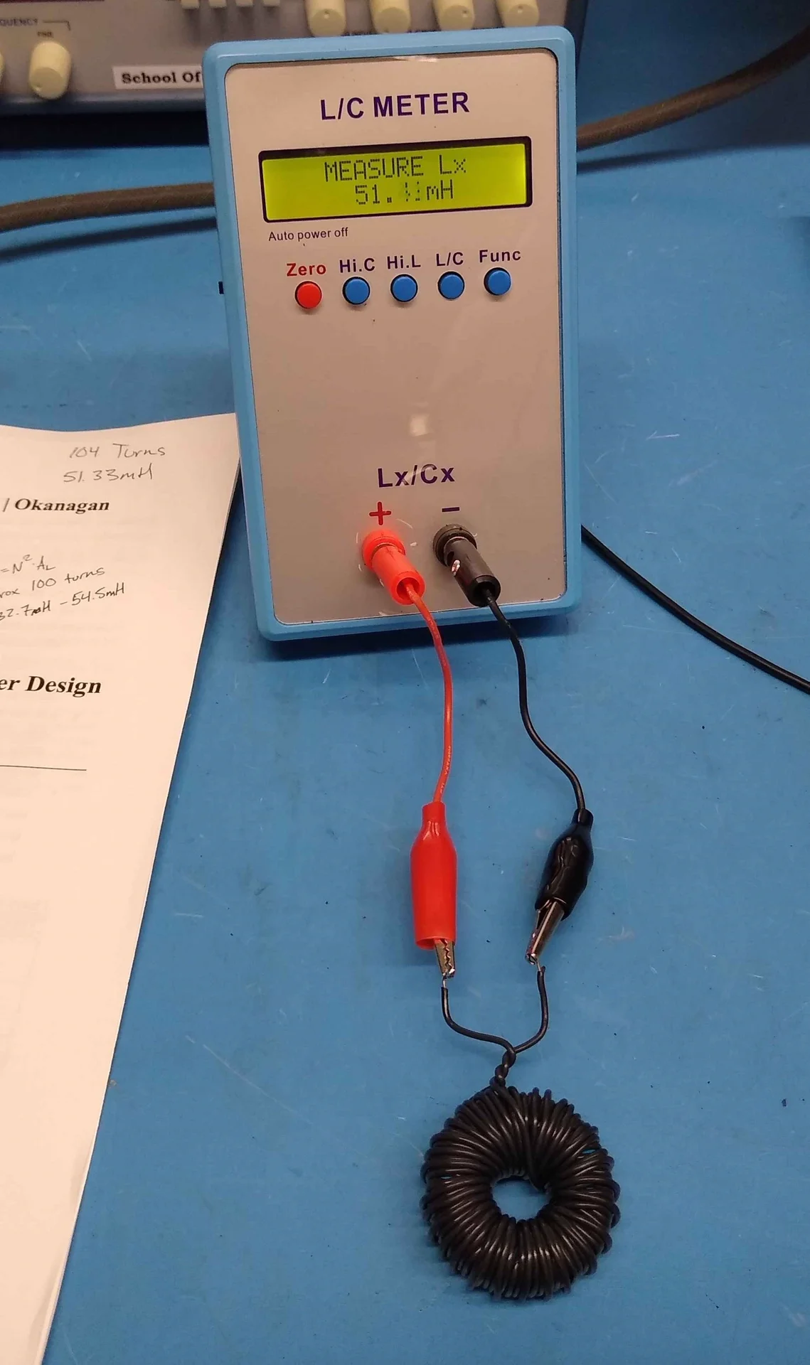
Breadboard Prototype
Once all components were prepared the MOSFET driver and boost converter circuits were prototyped on a solderless breadboard. To minimize parasitic resistances, switching noise, and EMI, which are common challenges in breadboard layouts, the high current transition ($di/dt$) paths connecting the power switch, rectifier diode, and filtering capacitor were kept as short and compact as possible.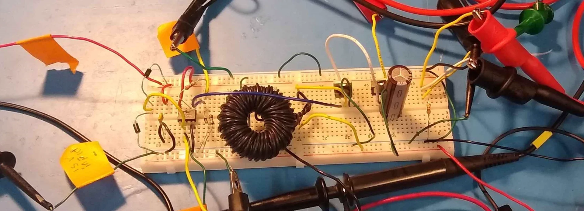
Measurements and Performance
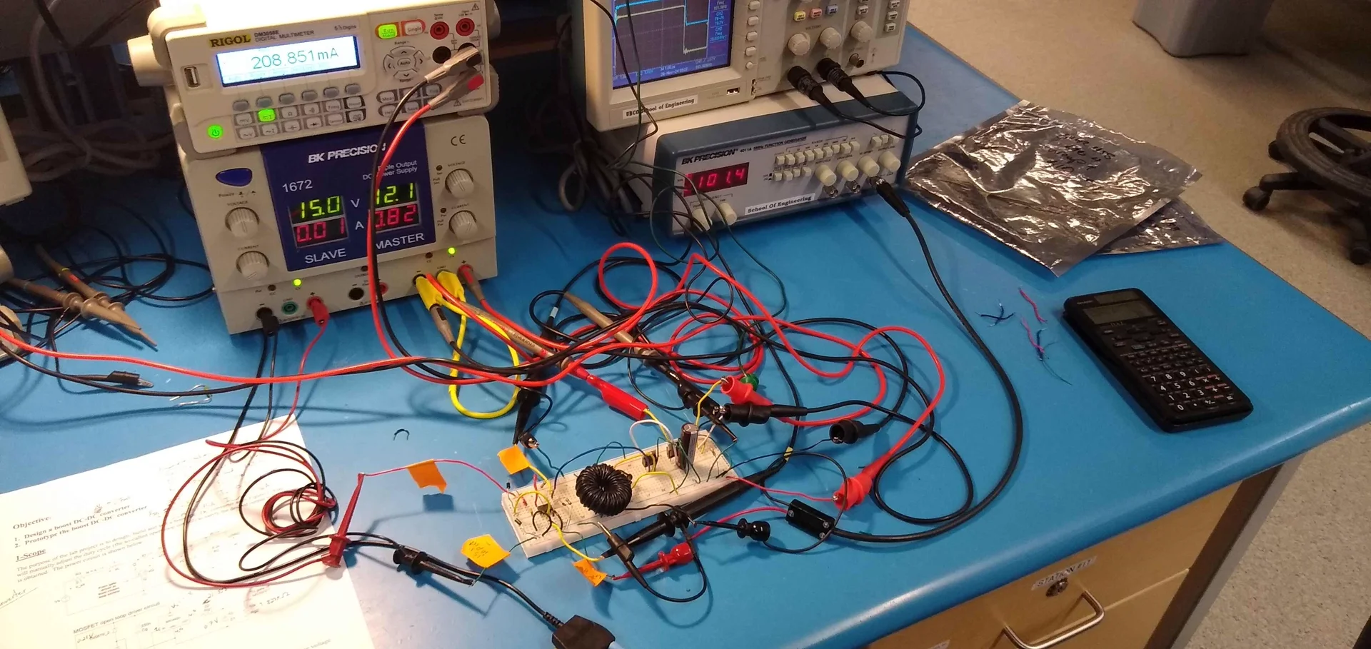
To make measurements on the circuit, we used a Tektronix TDS 2012B Digital Oscilloscope, Rigol DM3058E Digital Multimeter and BK Precision 2880B Digital Multimeter. Additionally, the function generator used to generate the 100 kHz switching signal was a BK Precision 4011A.
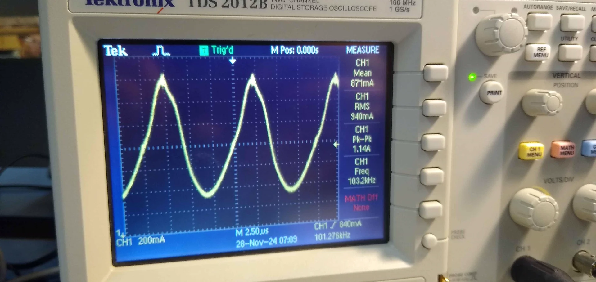
Following the lab manual, we first measured the voltage across the inductor which was about 48 V peak to peak. We then measured the current through the inductor as 0.940 $A_{RMS}$.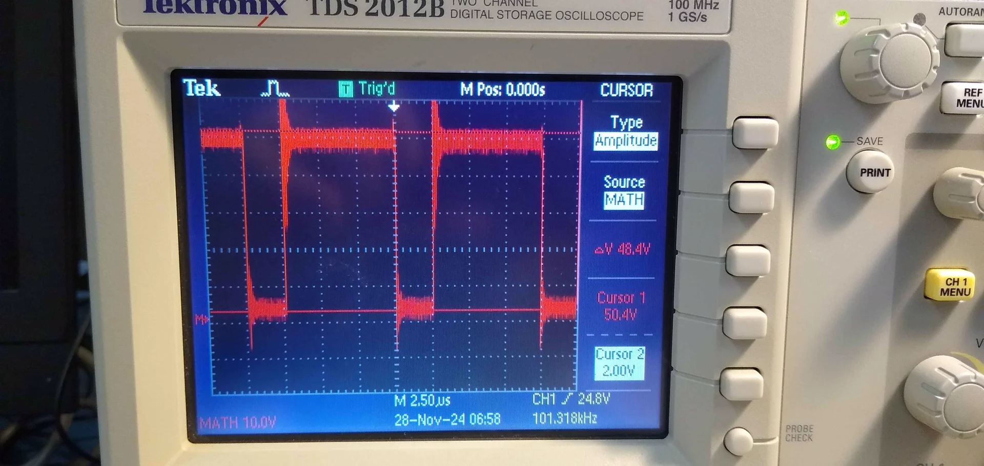
We monitored the active components by measuring the operational current waveforms of the MOSFET and the diode. The current through the MOSFET was measured to have 1.2 A running through it. The peak diode current was measured to be 768 mA.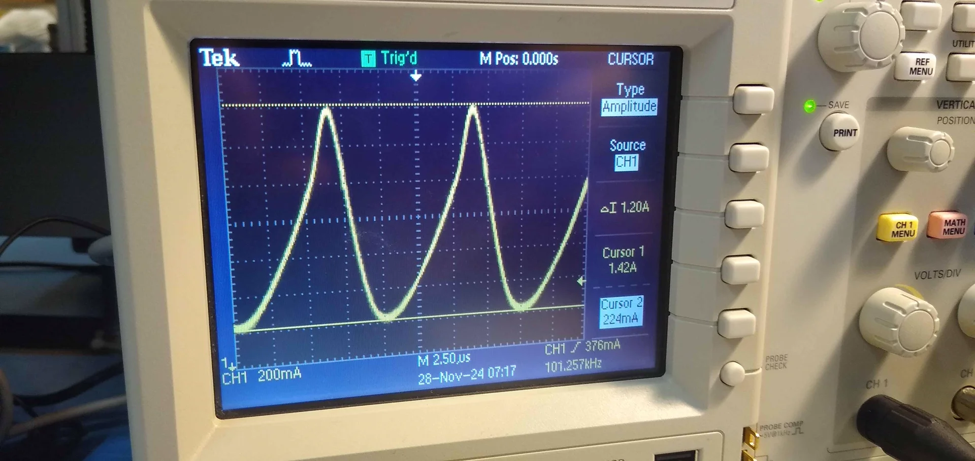
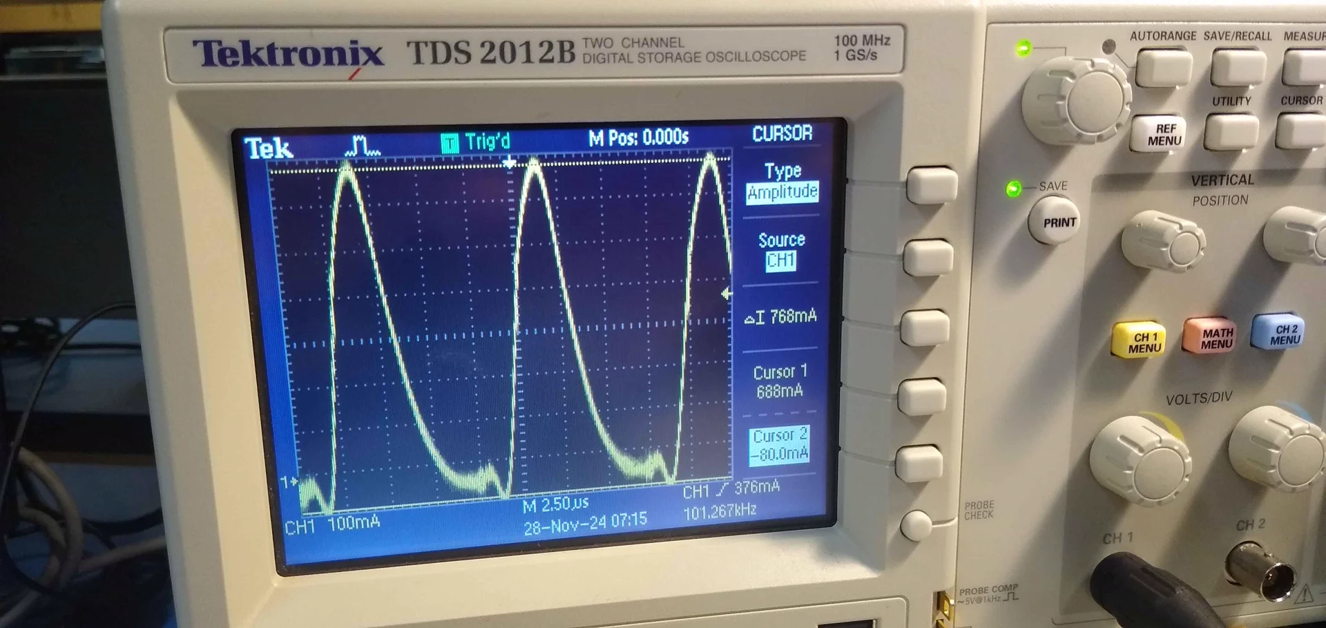
Capacitor current was also measured to evaluate the output stage. The peak current into the capacitor reached 768 mA, matching the peak forward current of the diode as expected from the circuit topology.
Finally the resulting voltage output was measured. Maintaining a duty cycle around 78%, we achieved a voltage output of 49.8 V given an input voltage of 13.3 V.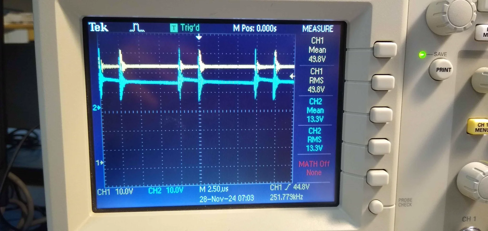
Challenges
One of the primary practical challenges during the build was managing voltage ringing across the MOSFET. The rapid switching transitions ($di/dt$) interact with stray circuit inductances and parasitic capacitances, creating resonant ringing when the device turns off. These voltage spikes can easily exceed the MOSFET's maximum drain to source voltage rating ($V_{DS}$). We verified this behavior by measuring the voltage waveform directly across the switch.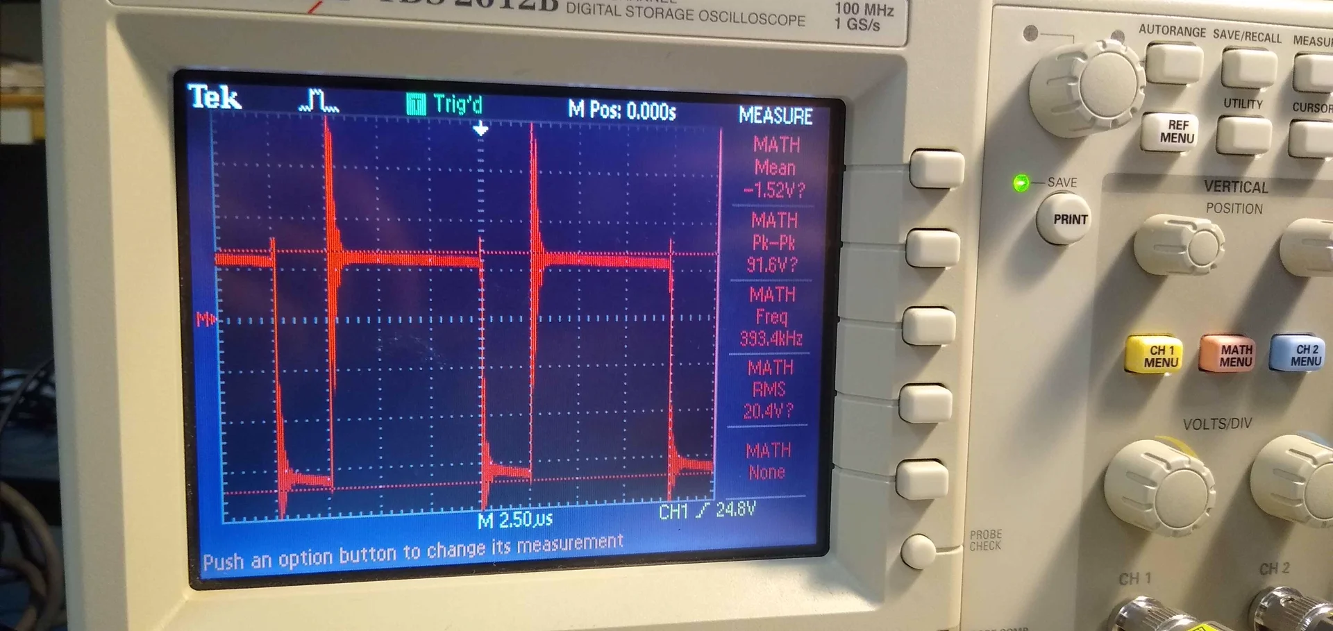
During switching transitions, excessive voltage ringing pushed the MOSFET dangerously close to its maximum breakdown voltage. A recommended future improvement is to integrate an RC snubber circuit across the power switch. The snubber would dampen the high frequency ringing caused by parasitic circuit elements, absorbing the transient energy and converting it to heat to protect the semiconductor from overvoltage failure.
Conclusion
This lab project provided an invaluable bridging experience between theoretical power electronics and practical hardware design. Building the circuit was highly engaging and personally nostalgic, reminiscent of an early high school project where I attempted to build a boost converter without understanding the underlying mathematics. While that early prototype worked largely by chance, this course has equipped me with the analytical tools to precisely calculate, model, and predict system behavior. Ultimately, designing and prototyping this 100 kHz converter served as excellent practice in component selection, layout optimization, and hardware debugging.