As part of the ENGR 352 Microelectronics II laboratory curriculum, we designed, prototyped, and evaluated a Photoplethysmography (PPG) circuit—a medical electronics device used to detect blood volume changes in tissue using optical sensors. While the baseline requirements were prototyped on a breadboard, the project offered a bonus opportunity to design and manufacture a custom Printed Circuit Board (PCB) for the completed system.
The development of the PPG circuit was systematically divided into four progressive stages:
- Sensor Stage: Integrating the optical sensor (the IR/Red LED and the receiving photodiode) to capture the raw biometric data.
- Transimpedance Amplifier: Converting the low-level current signal generated by the photodiode into a workable voltage signal.
- Secondary Amplification: Further boosting the signal amplitude and conditioning it to improve the signal-to-noise ratio (SNR).
- Signal Processing & Output: Implementing a differentiator circuit, a pulse generator, and an LED driver to cleanly turn the analog waves into distinct, visible pulses representing the heartbeat.
Initially, the entire four-stage architecture was successfully validated on a breadboard. Following this, the circuit was translated into a custom PCB design to secure the project's bonus credit.
PPG Design and Prototype
Building the Sensor
The sensor consisted of an infrared (IR) emitter, and an IR sensor. Using a piece of stripboard, we soldered the IR emitter and sensor to one end and wires to the other. This allowed us to
Transimpedance Amplifier
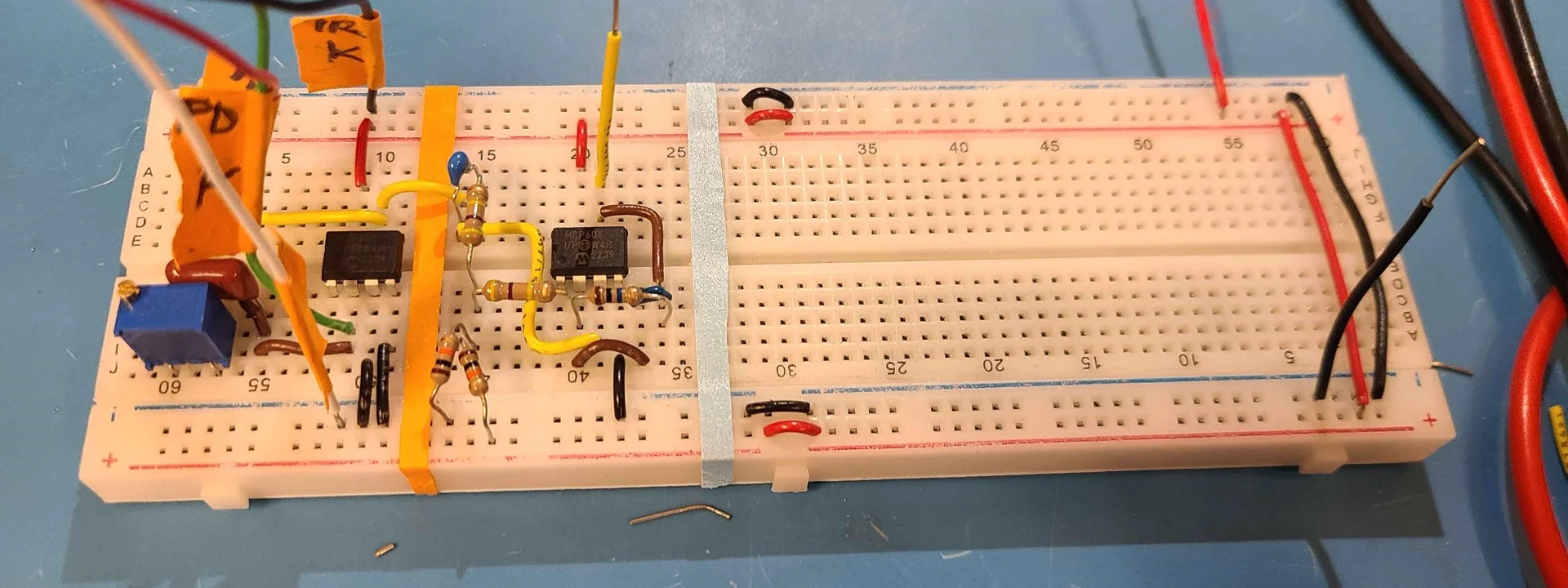
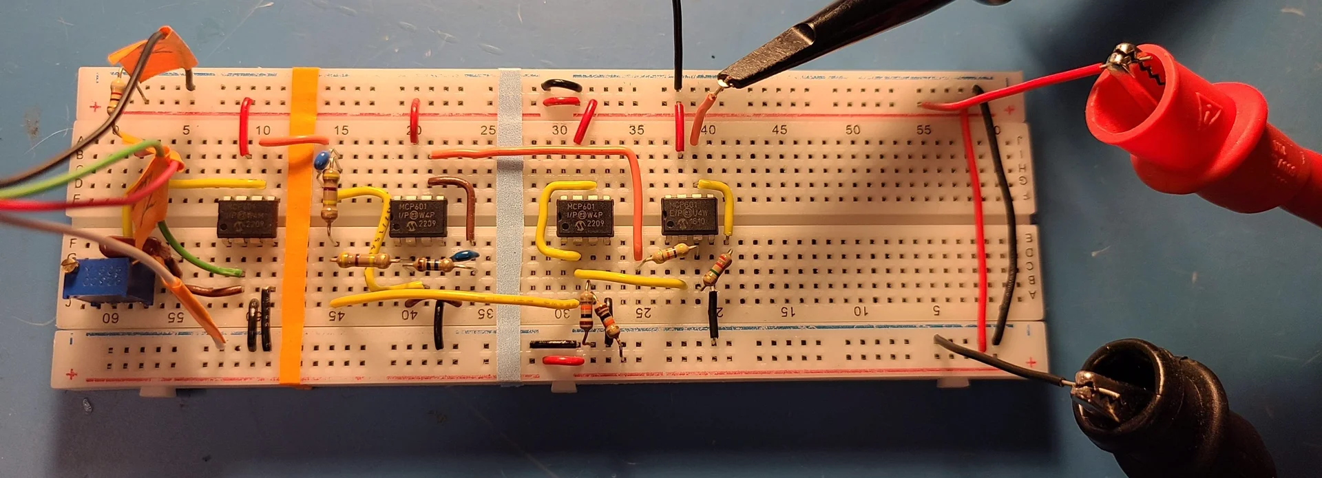
The transimpedance amplifier was simulated and built on a breadboard. The amplifier itself is built around the MCP601 Op-amp. An adjustable gain was implemented by utilizing a 5 Megaohm potentiometer as the feedback resistor. During the construction of the breadboard circuit, we adjusted the gain to achieve a decent level of amplification without saturating the output. In addition to the gain, a capacitor was added to the feedback loop to add some lowpass filtering around 12 Hz.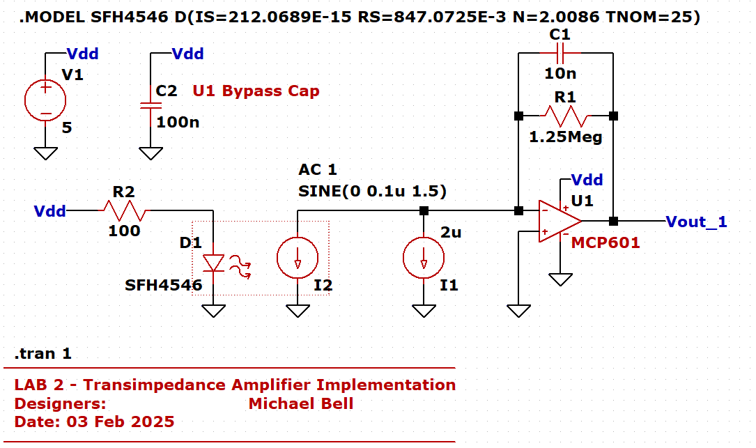
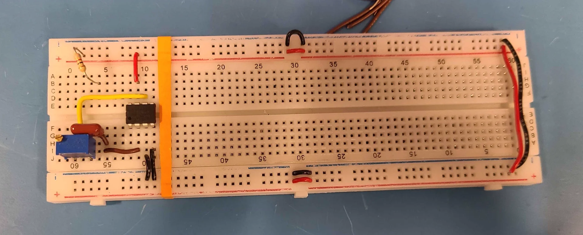
After the amplifier was built, we tested it for a signal. We were able to pick up our pulses.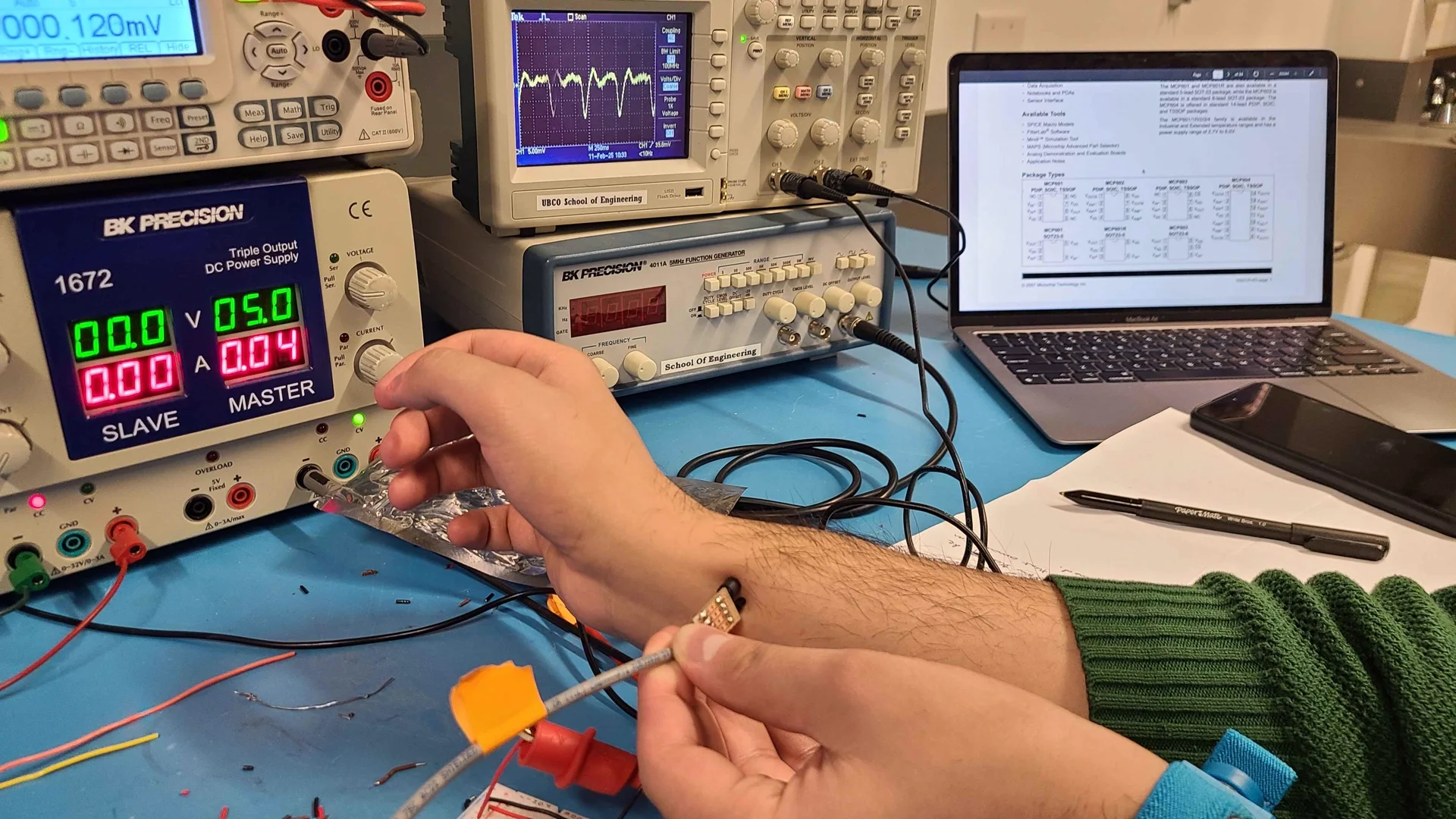
Second Amplifier Stage
The second amplifier was built using the same Op-amp as the first, but this amplifier utilized a non-inverting configuration with a virtual ground. The virtual ground allows for single-rail operation of the amplifier. The amplifier has a gain of approx. 21. The 4.7 uF DC blocking capacitor and 470 kohm resistor form a highpass filter centered around 0.072 Hz, and the 1000 pF capacitor in the op-amps feedback loop (along with the 10 Mohm resistor) form a lowpass filter around 16 Hz.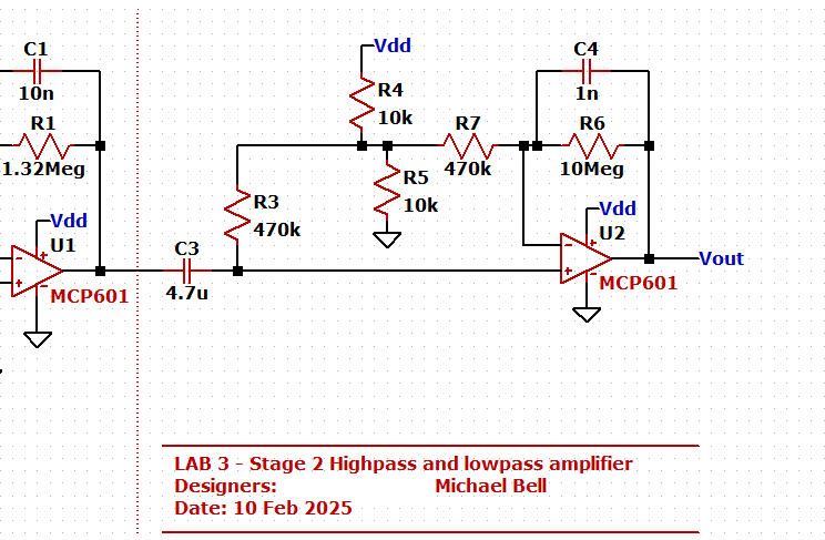
Once again, after the breadboard circuit was constructed, we tested its operation.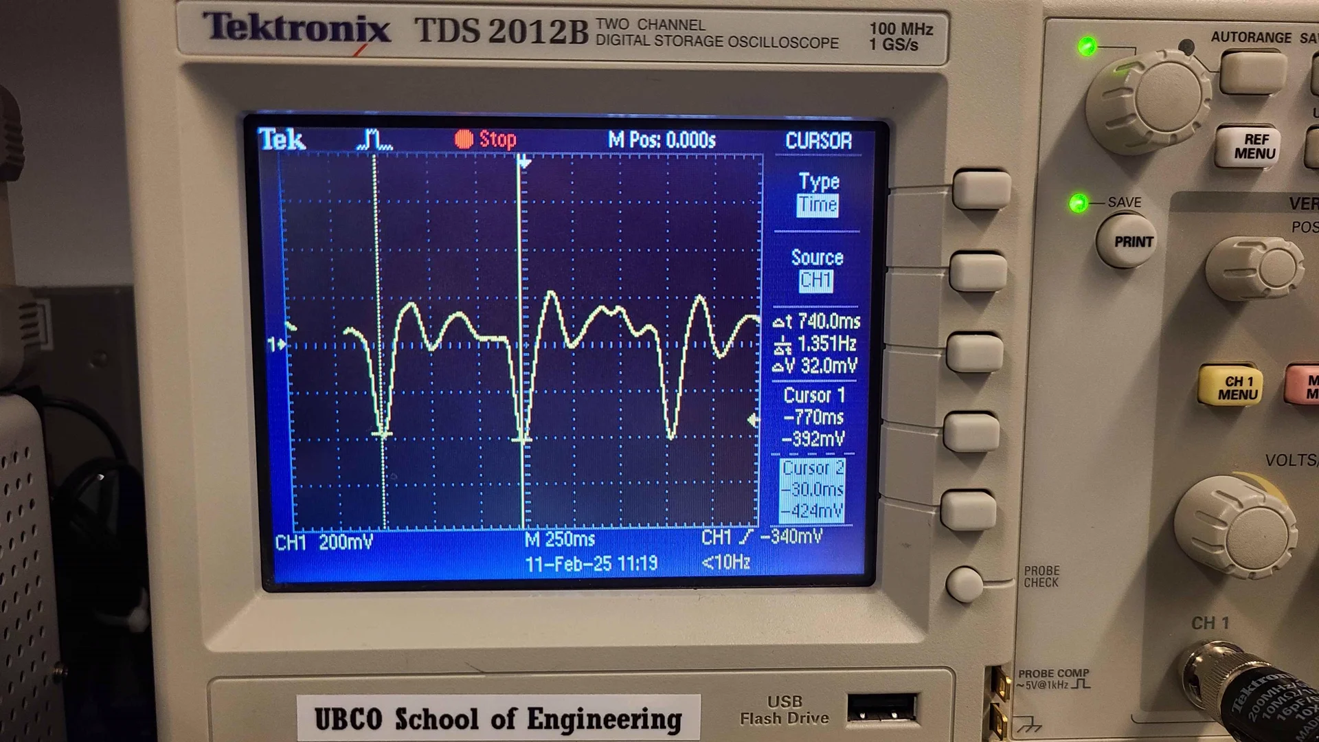
Comparator with Hysterisis
After the second amplifier, a comparator was added to convert the analog PPG signal into a discrete pulse that can be used for any number of applications. In the design of the comparator, positive feedback was added to create some hysterisis in the circut. This hysterisis prevents small variations near the threshold voltage from creating noisy pulses by seperating the high threshold and low threshold.
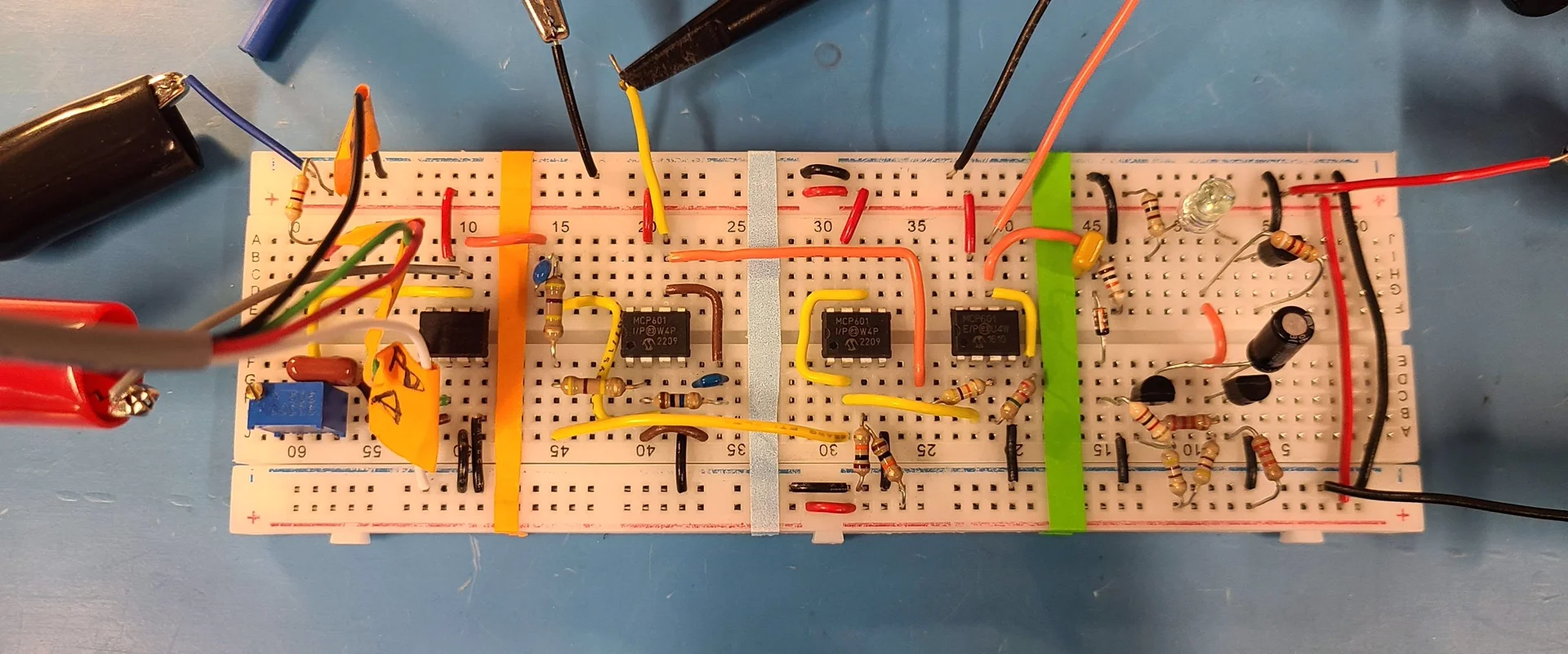
The comparator circuit was drawn, simulated, and built on the breadboard alongside all other components as shown below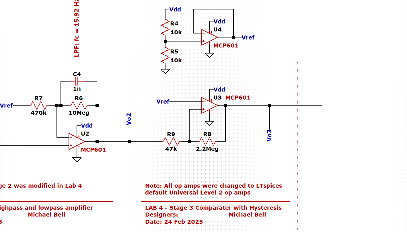
The circuit was tested and operated as expected. Comparator test video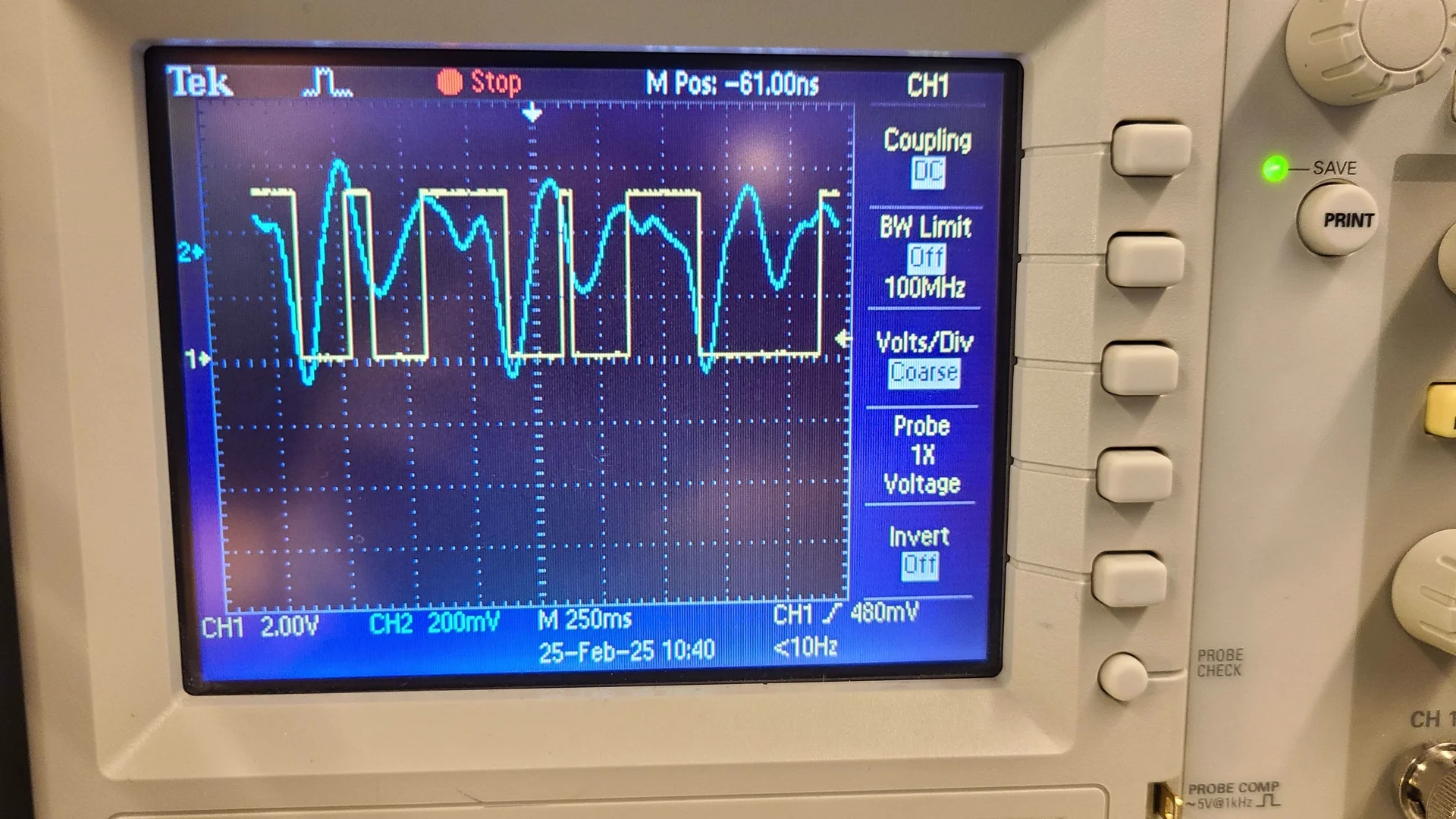
Differentiator and Pulse Generator
The final stage(s) of the PPG circuit were the differentiator, pulse generator, and LED driver. The differentiator consisted of a capacitor, diode, and two resistors. The capacitor is the main component that differentiates the sharp comparator edges into positive and negative pulses. The diode then only allows positive edge signals to go through. The shunt resistor on the anode of the diode is to provide a ground path for negative pulses. The positive edge then triggeres a monostable multivibrator. The monostable multivibrator produces a precisely timed pulse given and input trigger. This timed pulse then lights an LED.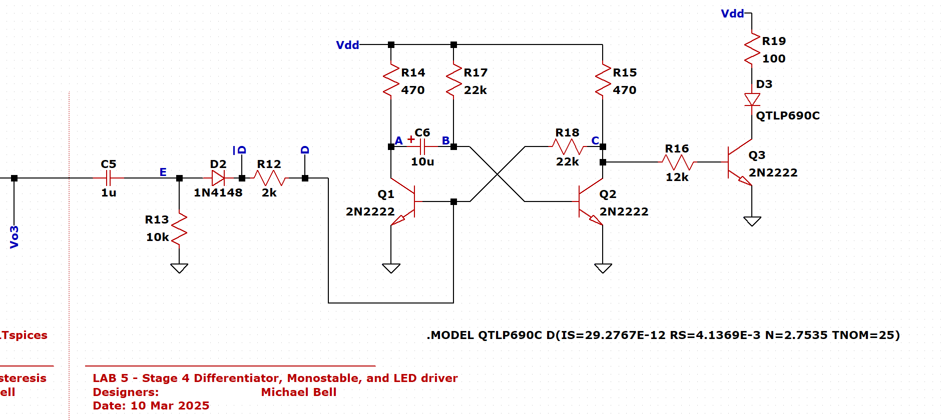
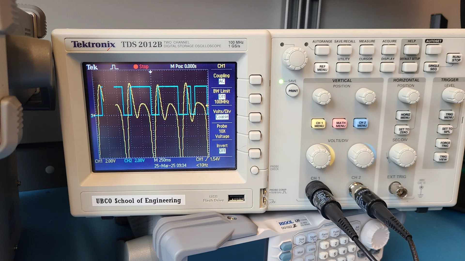
Testing the differentiator first, everything functioned as intended. The output of the diode marked with the D_bar is the yellow trace (ch1) and the 2k resistor output D is the blue trace (ch2).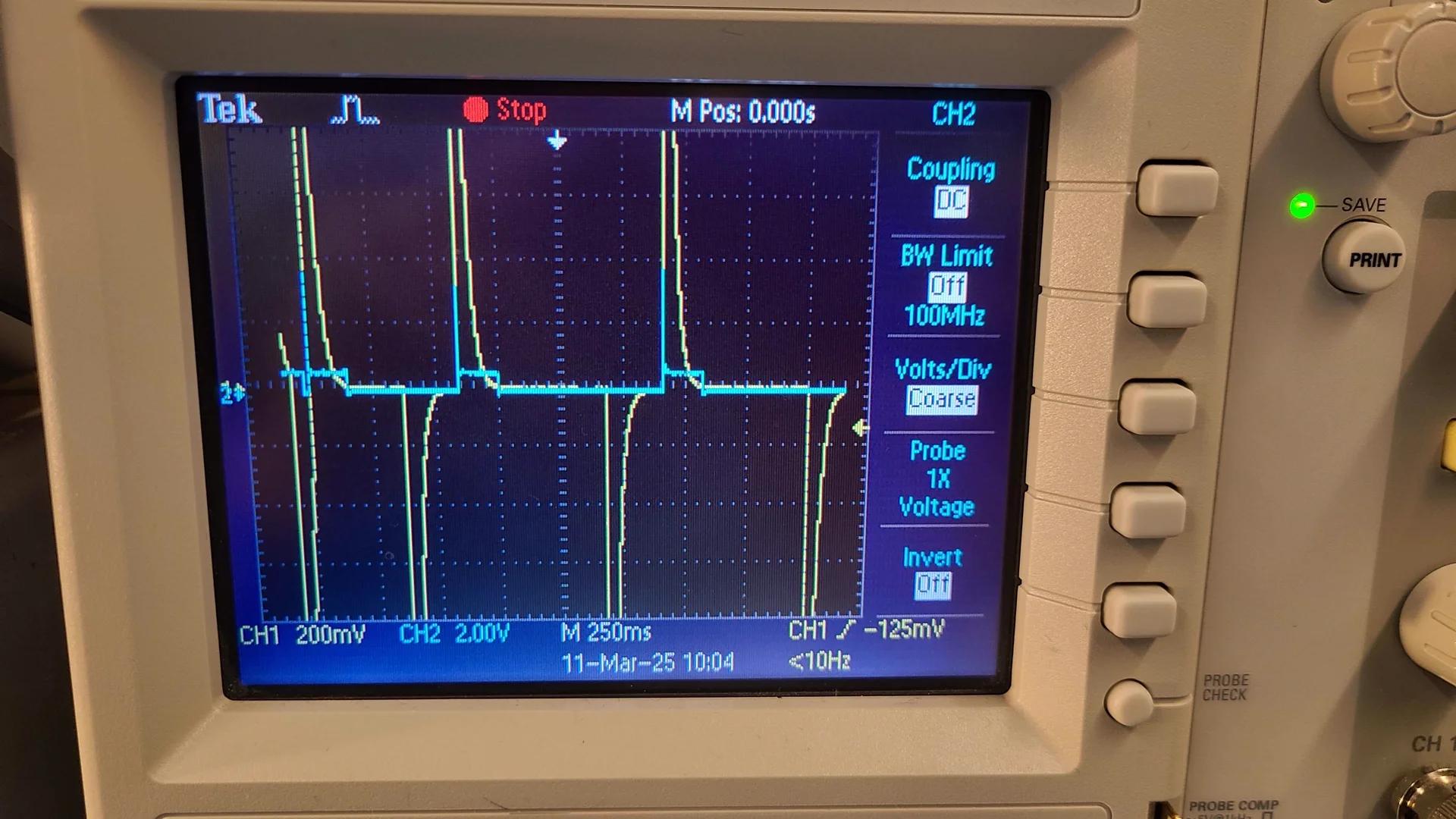
Next the output of the second stage amplifier (yellow ch1) and pulse generator (blue ch2) are shown, giving a clean representation of the analog PPG signal and digitized LED output signal. Pulse generator video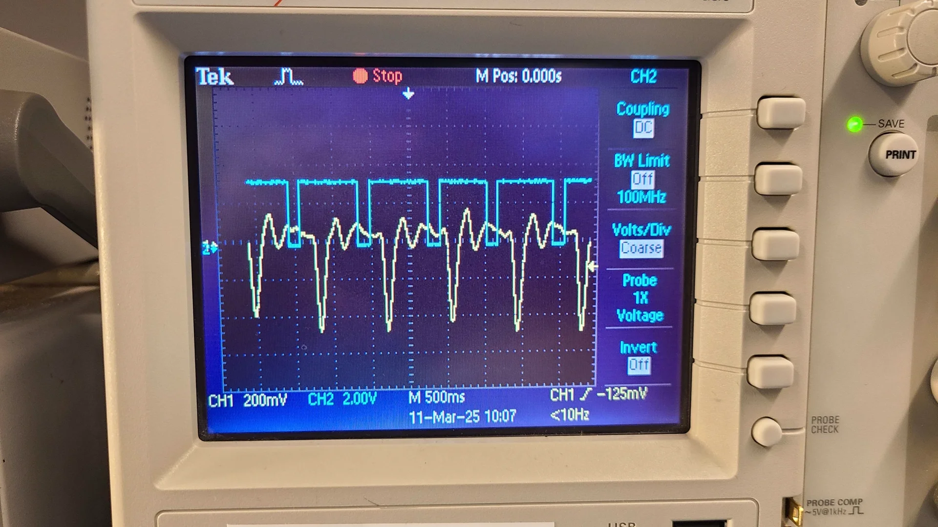
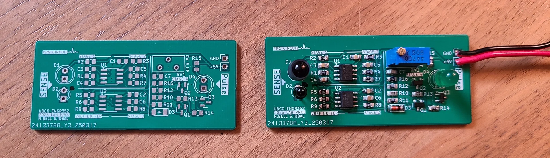
PCB Design and Part sourcing
With the prototype built, the schematic and PCB were designed in KiCad. Parts were sourced from Digi-key with all passives being in the 0805 SMD package for ease of soldering. The dual package SOIC-8 variant (MCP602-I) of the op-amp was chosen.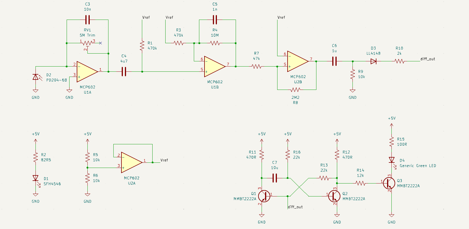
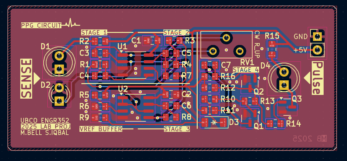
The board was then sent to be manufactured.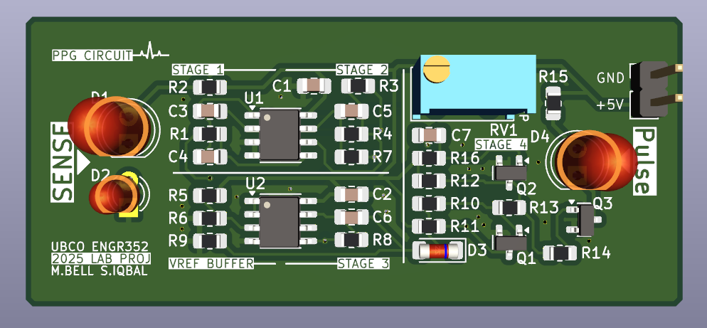
Results
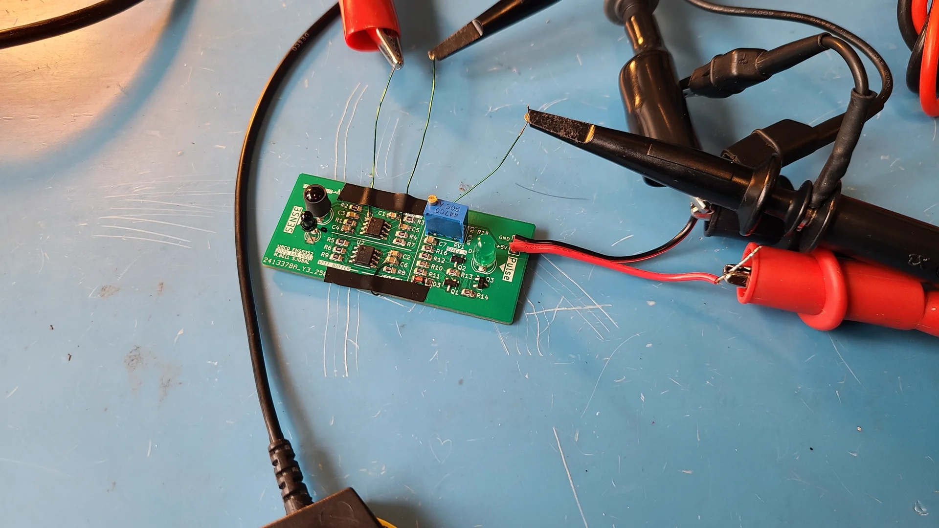
Once the components and PCBs arrived, the boards were populated and prepped for testing. Because test points were accidentally omitted during the design phase, we improvised by soldering 28 AWG magnet wire to the board to act as manual probes. Fortunately, this workaround worked perfectly, and testing proceeded smoothly.
Cost Analysis
The total cost of the project came to CA$80, broken down as follows:
- PCBs: ~CA\$40 (the boards themselves cost less than the shipping).
- Components: ~CA\$40.
While the overall budget was a bit higher than anticipated, this was primarily driven by a few specialized, pricey components—most notably the 5 MΩ potentiometer.
Final Takeaways
In the end, the project was a resounding success. The final results were fantastic, the hardware performed beautifully, and the hands-on troubleshooting provided some incredibly valuable lessons for the next design iteration.