During my Undergraduate Capstone Project, my team realized that there were no devices that we could test our newly designed Ku-band scalar network analyzer (SNA). Because of this we needed a device that operates around 15 GHz to be able to compare and test our SNA with, all within 24 hours.
Using the AWR Microwave Office software I set out to design a Split Ring Resonator (SRR) notch filter.
A SRR functions the same as a resonant LC tank circuit, where the conductive loops provide inductance (L), while the gaps provide capacitance (C). When an oscillating electromagnetic field is present parallel to the SRR, it induces a circulating current producing resonance at a frequency determined by the L and C values.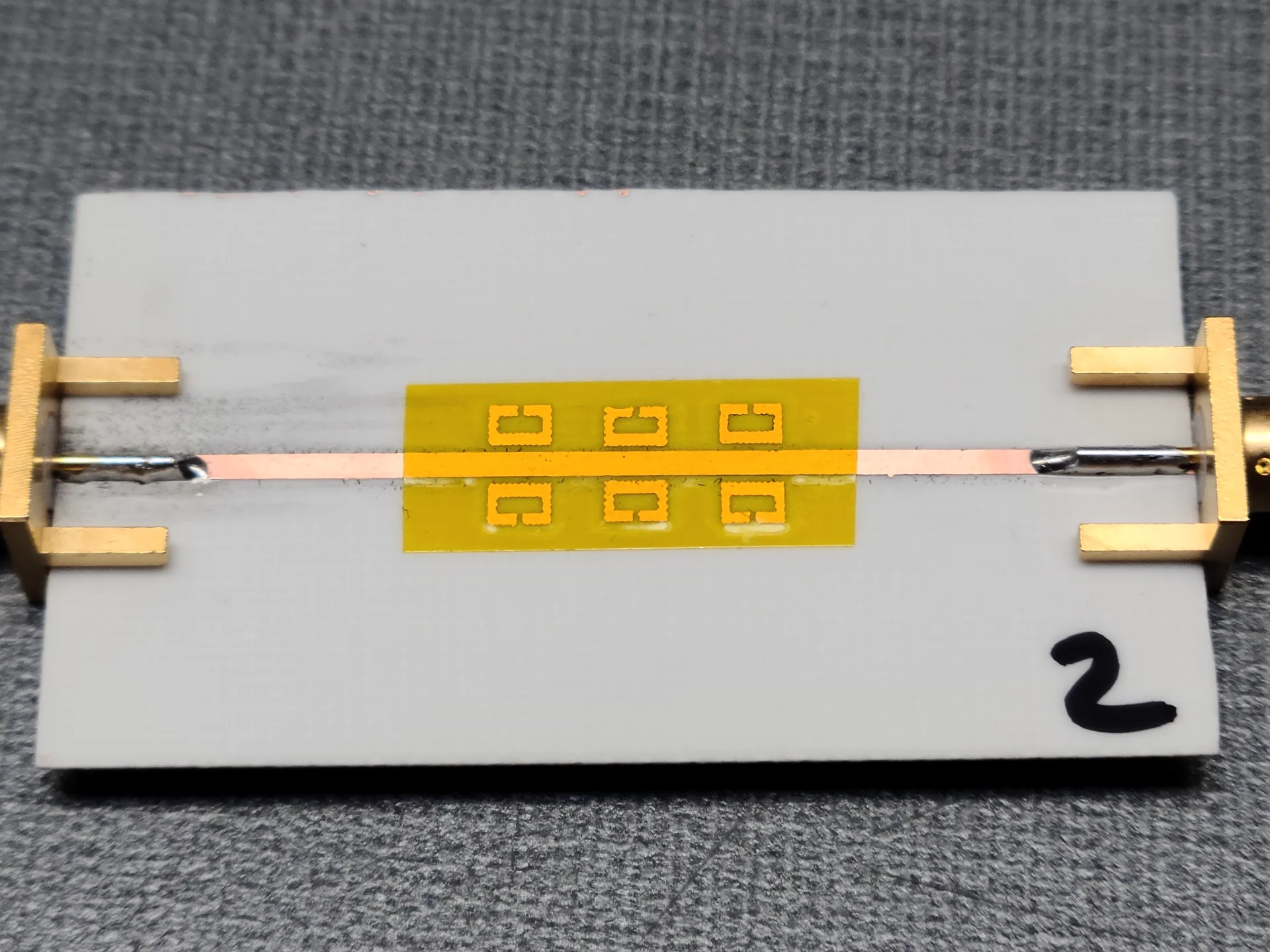
Design and Simulation
To start the design process, I created the basic shape of a SRR. The dimensions of the ring were set to ensure the overall ring length was a one-half wavelength of the resonant frequency as recommended by the graduate student I was working with. In the case of 15 GHz, the overall length of the SRR should be 10 mm (which is quite small).
For this design I chose to placing the SRR's parallel to a microstrip transmission line. Doing this will create a notch filter centered at the SRR's resonant frequency. While the length to height ratio of the SRR isn't critical, I made sure that the length was longer to better couple with the transmission line. To tune the SRR I took an iterative approach, changing one variable at a time and running a low-precision simulation. This simulation helped locate the resonant frequency to ensure I was on the right track.
Transmission line
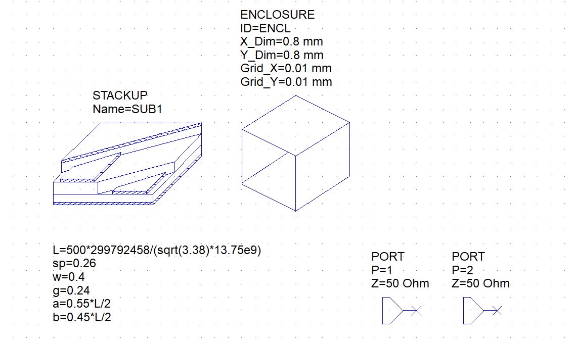
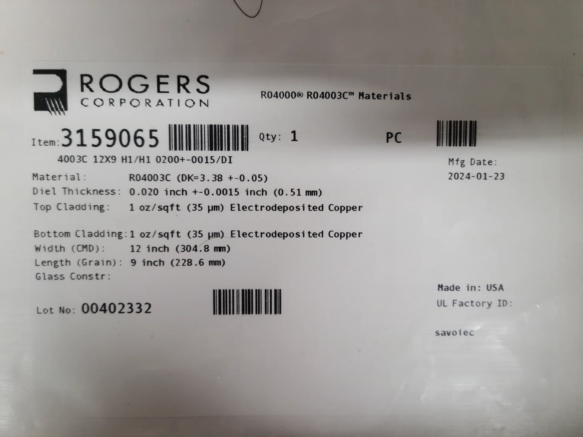
To design the transmission line I used AWR Microwave Office's built in TXLine tool. With this tool I calculated the dimensions required for a 50 ohm 15 GHz microstrip transmission line on a Rogers RO4003C substrate. The substrate was 0.51 mm thick with a copper thickness of 35 um. From the TXLine result, a trace width of 1.156 mm is required.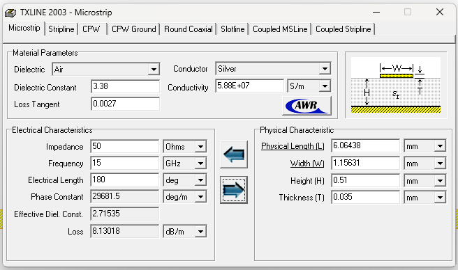
Initial Design
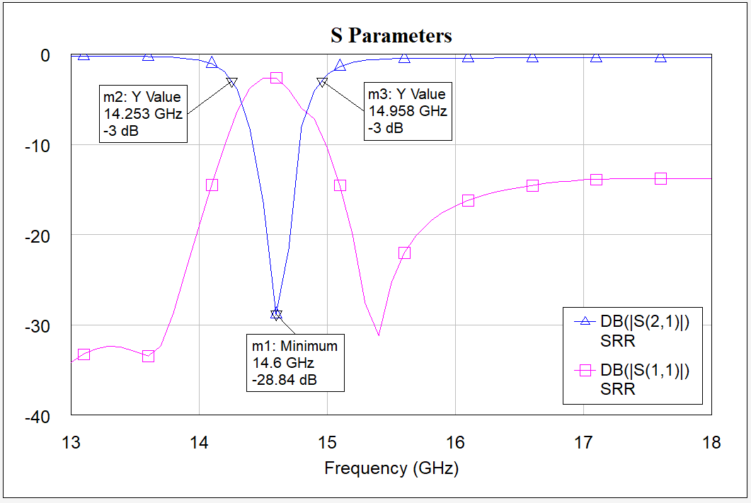
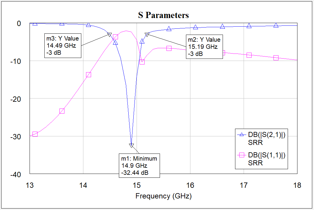
In the first design I ran a quick simulation with 1 SRR, and decided to use 6 SRR's on one line to achieve the desired notch magnitude (depth) at the resonant freuqency. The resulting Q-factor of the notch was around 21, with a bandwidth of 705 MHz. This was good, but it wasn't at the target frequency and I wanted a wider bandwidth so lower-resolution network analyzers can see the notch.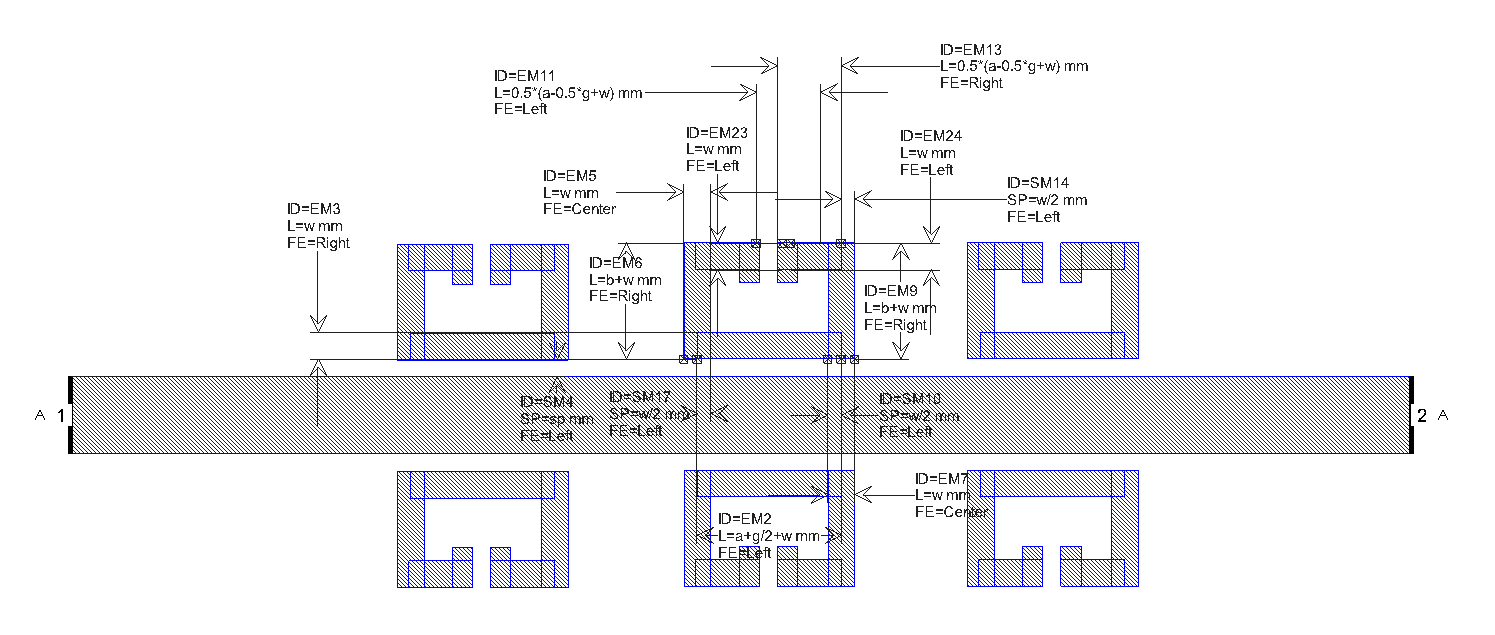
Tuning the freuquency
Continuing with my iterative design approach to this, I started adjusting portions of the SRR to achieve different results. To do this I went back to using 1 SRR and ran some courser simulations. I found that by making the bottom length of the SRR thicker, I could achieve the frequency I wanted to design to, as well as improve the notches magnitude.
For the single SRR, the frequency was centered at 15 GHz and had a Q-factor of 60. The geometry of the SRR was 0.25λ tall by 0.3λ wide, a trace width of 0.4 mm with the bottom trace being 0.6 mm, a gap of 0.25 mm, and 0.23 mm spacing from the microstrip.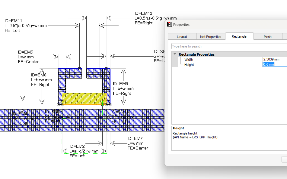
I wanted to see if I could improve the depth of the notch so I placed 6 SRR's on the microstrip again. This time the notch was much deeper and still on frequency, with a bandwidth of 700 MHz and a Q-factor of 21.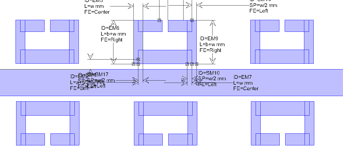
Increasing the Bandwidth
Satisfied with the depth of the notch, I began testing ways to increase the bandwidth (lower the Q-factor). The best simulation results I achieved were after spacing the SRR's 2.33 mm from each other and increasing the outer SRR's spacing from the microstrip by another 0.1 mm (making it 0.3 mm). I achieved a bandwidth of 701 MHz (marginal if any improvement at all) and a notch depth of -28 dB.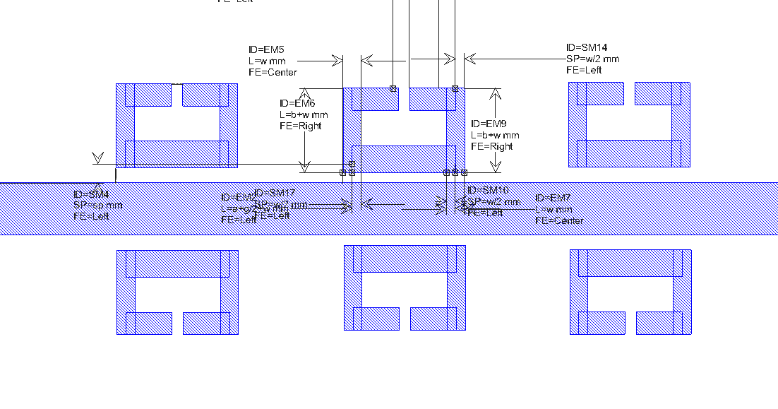
After spending some time simulating different configurations, time was running out so I settled for the 700 MHz bandwidth.
SRR PCB Fabrication
I translated the design from AWR Microwave Office to KiCad to generate the necessary PCB fabrication files. I designed the SRR around the Rogers RO4003C substrate.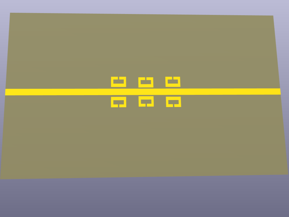
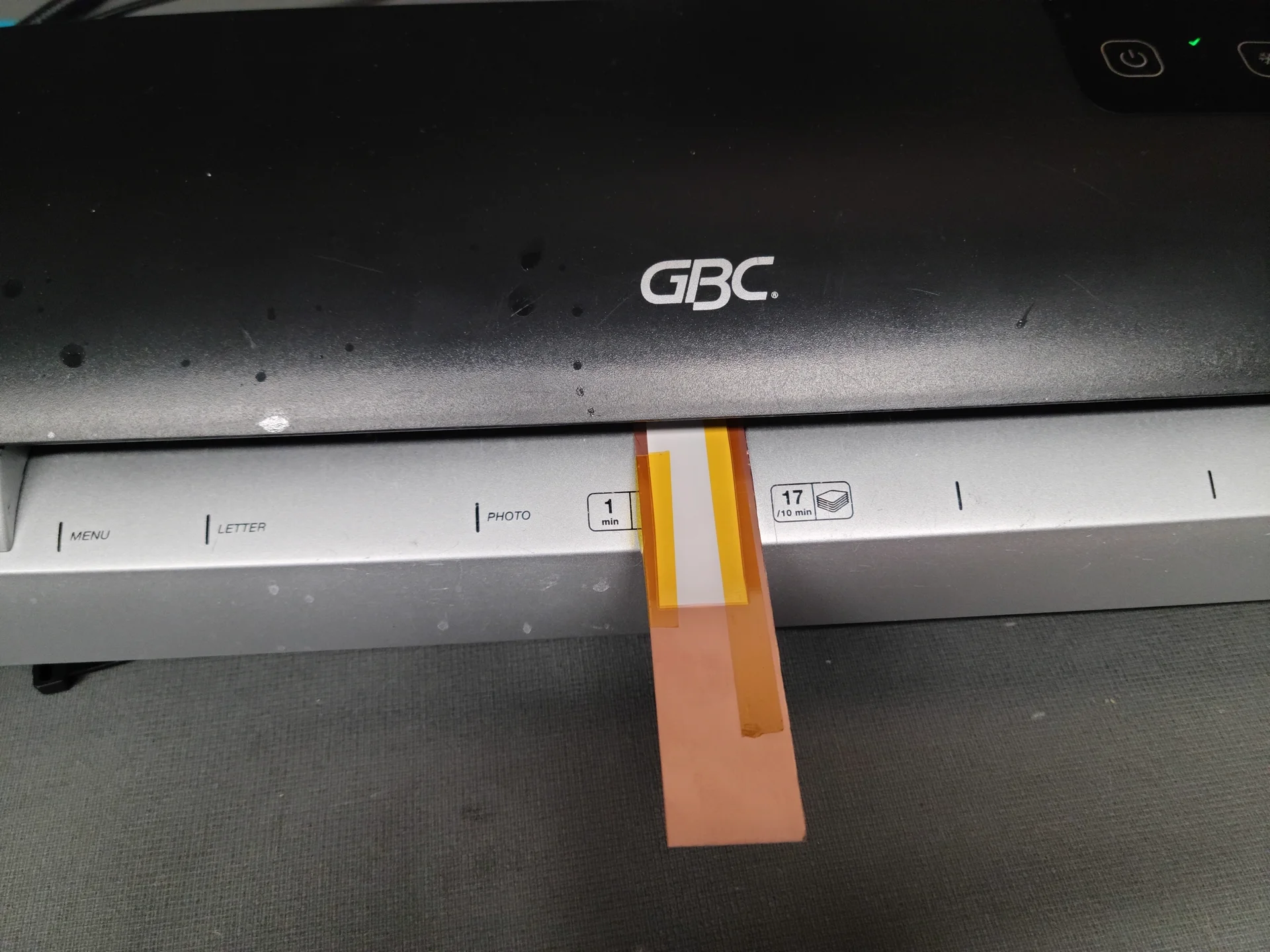
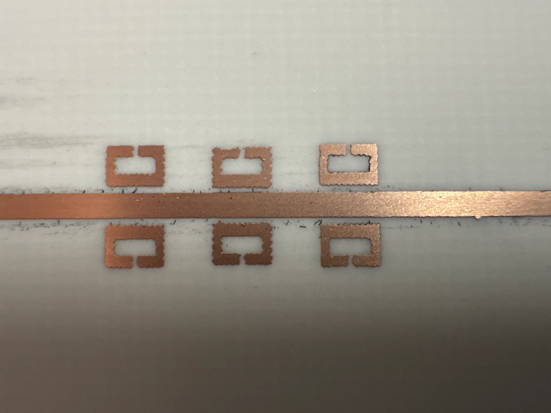
Using a 1200 DPI laserjet printer, I printed the PCB design on to some gloss paper. I then used a laminator to transfer the toner from the gloss paper onto the RO4003C copper clad board. After the toner is transferred to the copper clad board, I tape off the back side to keep the copper ground plane and etch the board in ammonium persulphate.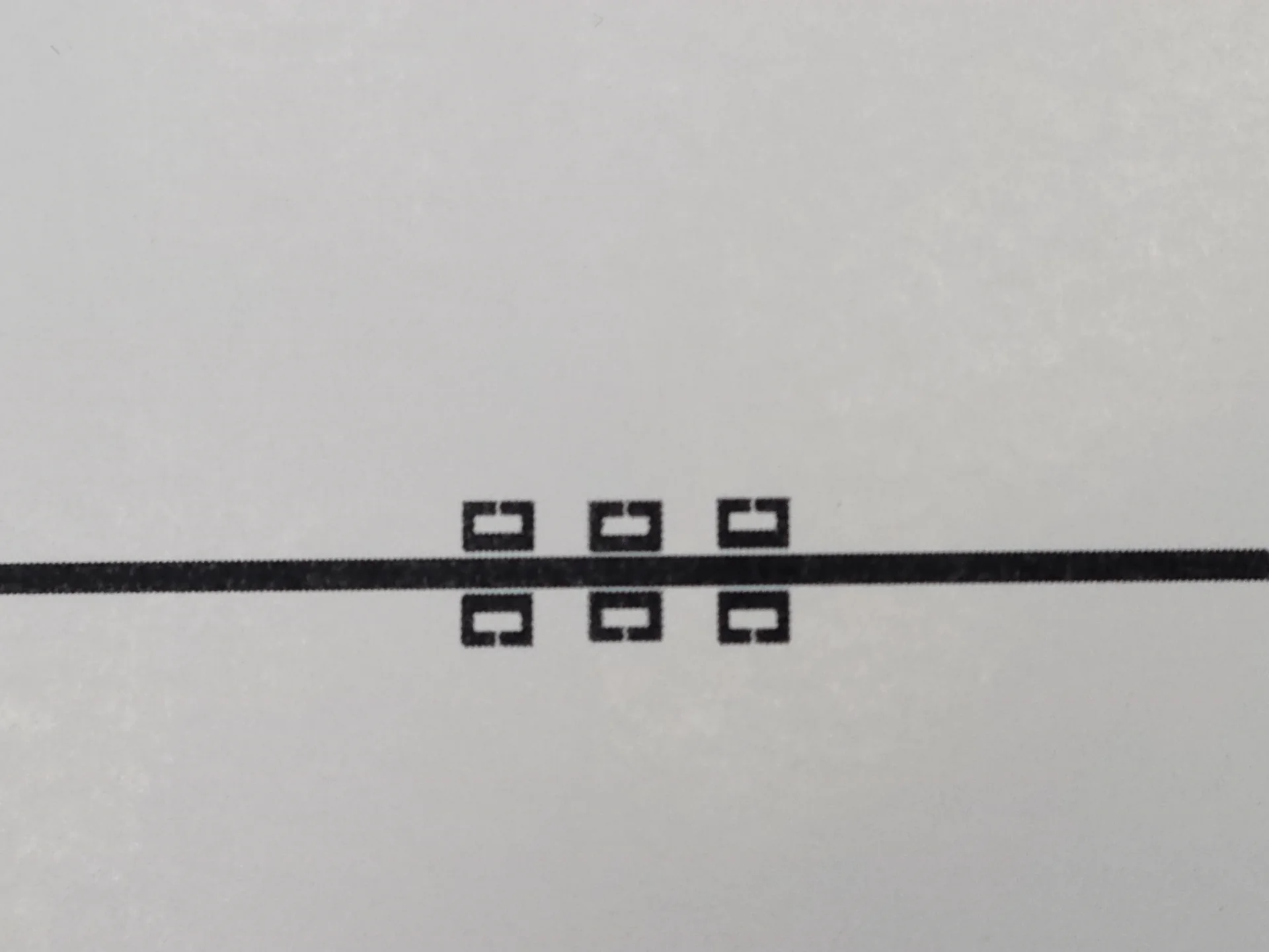
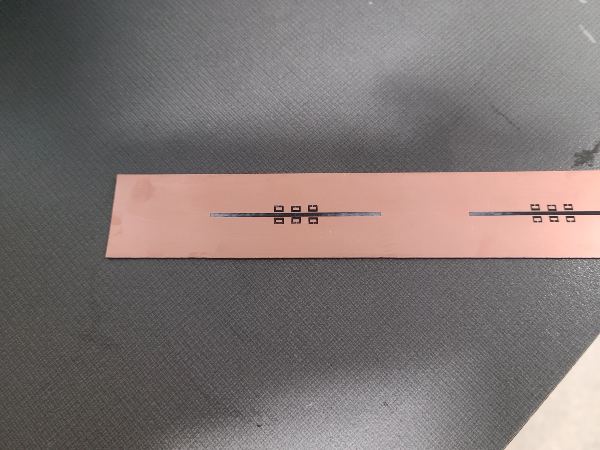
The results after the etching process were promising. The SRR dimensions were on the edge of the printers resolution, so the resulting PCB had "bumpy" traces.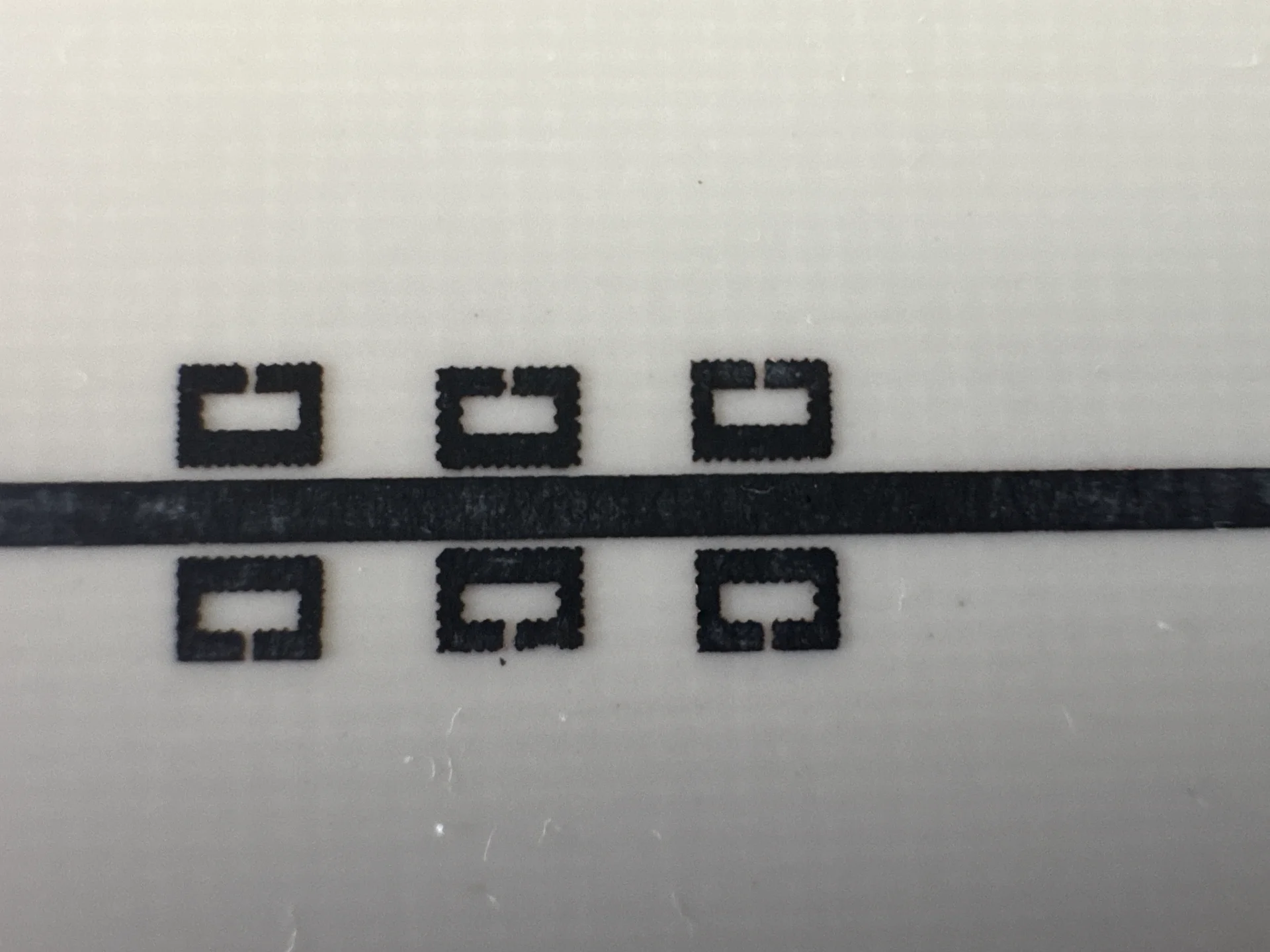
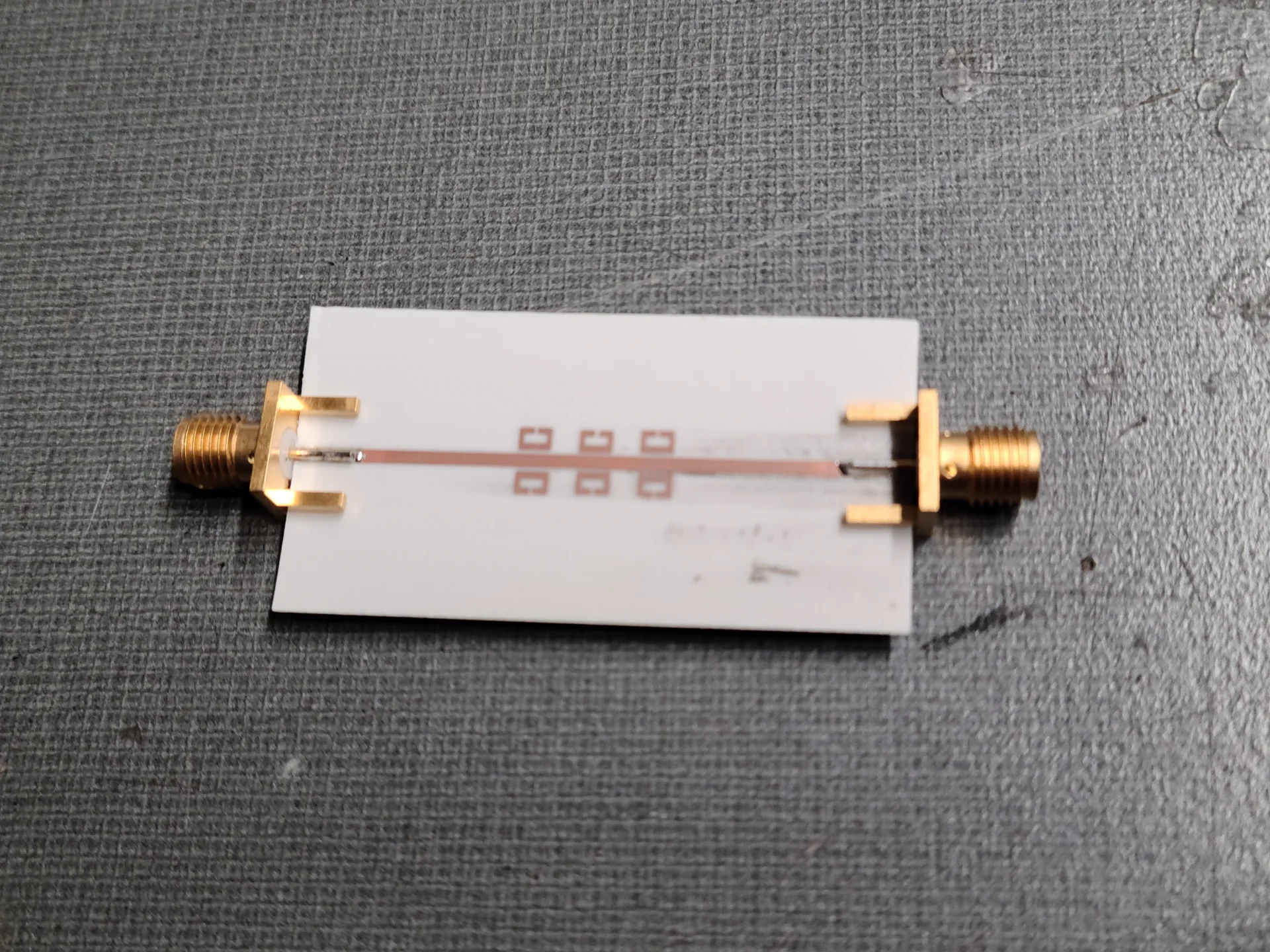
Lab tests on Keysight N5222B PNA
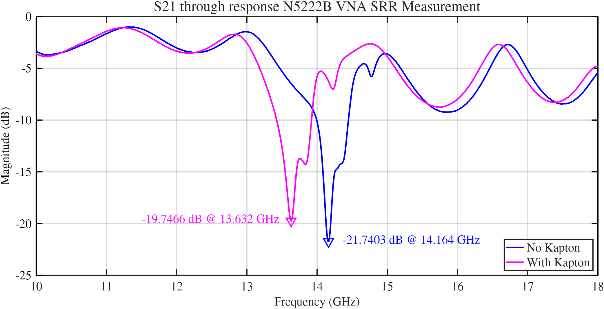
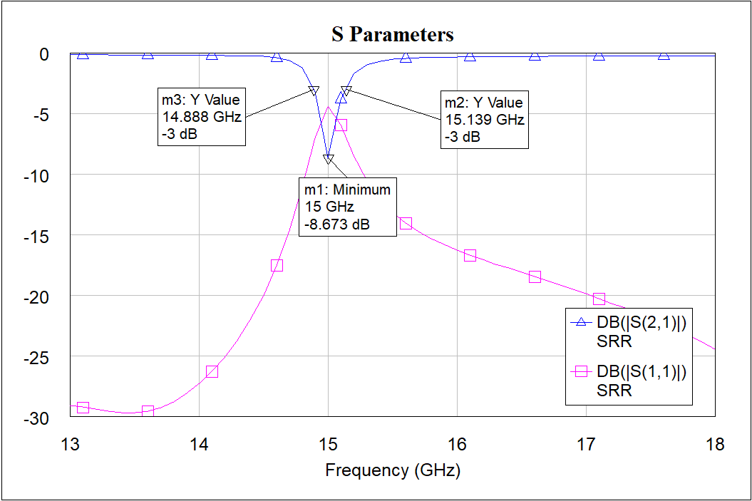
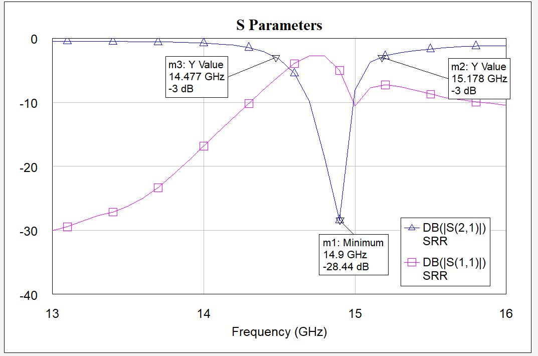
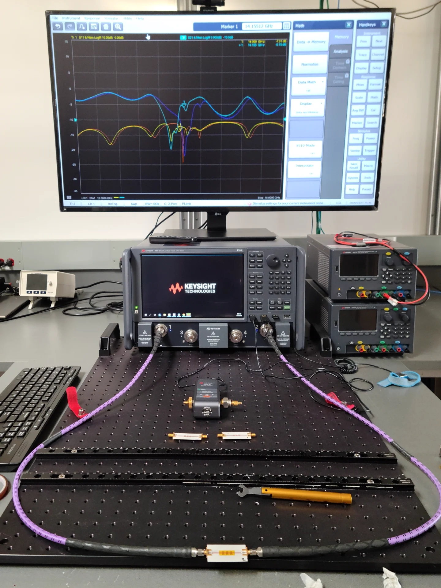
After fabricating 3 of the SRR PCBs, I tested them from 12-18 GHz on a calibrated vector network analyzer. The results of which were close to what I designed, but off from the initial frequency. I tested the SRR on its own and achieved a notch at 14.155 GHz, and a depth of -21.75 dB. Curious, I then placed some Kapton tape over the SRR's to see what it would look like. Shown in the second image, the S21 measurement of the SRR with Kapton is shown in bright blue, while the SRR without the Kapton is shown by the dark blue trace.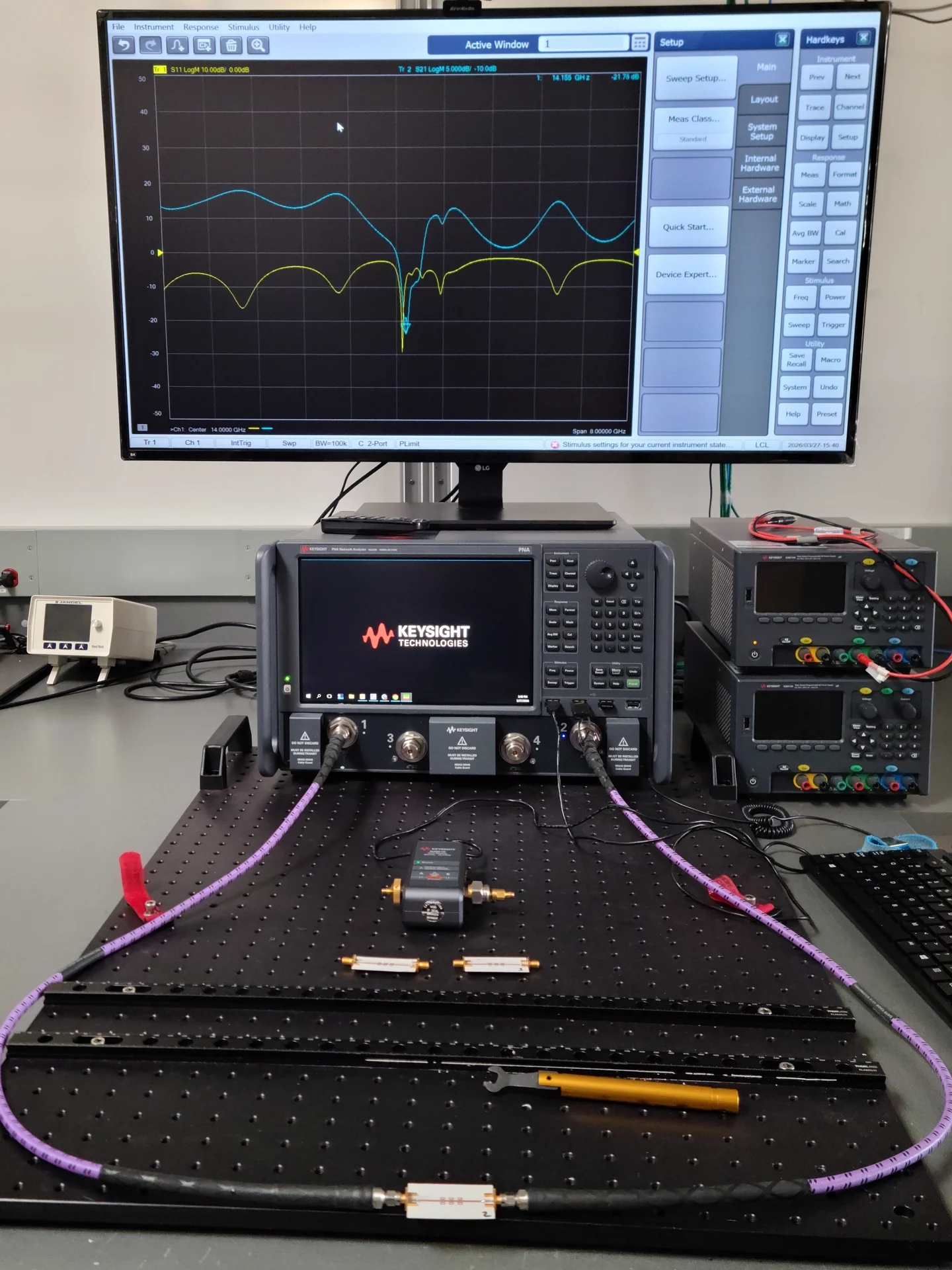
Results and Challenges
This project was a means to an end, with the main purpose being to test the scalar network analyzer (SNA) my team and I designed for our undergraduate capstone project. We measured our SNA using the SRR with the Kapton tape.
The key challenge in making this SRR was managing the sizes of every trace. Striking a balance in trace width, spacing, gap width, and overall dimensions was a hurdle that took lots of iteration. Being limited in time, continuously running simulations for each iteration would take too long, so I strategized. Utilizing patterns I notice with each simulation, making educated changes based on those patterns, and running low-resolution simulations allowed me to optimize the time it took to design the SRR filter.