Undergraduate Engineering Capstone
Engineering capstone is the final undergraduate engineering project students complete in their undergraduate degree. Teams of 6 to 7 students are assigned a project provided by local industry partners or university faculty and completed over the span of their final year (2 terms).
The project assigned to my team was titled "Development of miniaturized readout electronics for microwave ice sensing applications in harsh environments".
Project Overview (The Why)
Ice buildup is a serious issue in aerospace and wind energy systems, where accumulation can reduce aerodynamic performance and create safety hazards. Our capstone project focused on designing a portable Scalar Network Analyzer (SNA) capable of detecting ice using microwave resonant sensors. The device measures shifts in resonant frequency from Split Ring Resonators (SRRs), allowing ice formation to be detected in real time. The objective was to create a lightweight, field deployable alternative to traditional laboratory network analyzers for use in wireless microwave sensor networks.
The project was initially defined through its proposal and later expanded upon by our client Dr. Mohammad H. Zarifi. Project Proposal Problem statement - What is the Problem that this project is meant to solve? Microwave resonant sensors are low cost and simple to fabricate for many different applications. However, current microwave readout electronics can be expensive, heavy, and implement many features so they are useful in a variety of different applications. This project will focus on readout electronics specialized in measuring the necessary response from microwave ice sensors. This will miniaturize the electronics required for ice sensing to provide more flexibility on use and portability, such as drones for ice sensing automation. This technology can be used to create safer infrastructure and improve safety for maintenance workers. Background - Please provide any additional relevant background information that is related to the problem you would like this project to solve. This project involves designing and development of a two-port circuit implemented on a printed circuit board (PCB), capable of characterizing the frequency response of a resonator within a limited frequency range, dynamic range, physical dimensions, and weight. The system will be integrated wirelessly with smart devices or portable electronics for visualization and communication purposes. Constraints - What are the Constraints for the problem you are trying to solve? The objective of this project is to design, build, and implement a scalar network analyzer capable of measuring the amplitude frequency response of resonant based microwave sensors, while being low weight and maintaining a small form factor. Since this device will be implemented in ice sensing projects, the device is expected to withstand temperatures below zero; because of this, the device must remain operational and accurate for temperatures as cold as -40℃ or as hot as 60℃ with a frequency range between 1 to 8 GHz, dynamic range of 50 dB or more, and minimum output power of –5 dBm. Risks - What are potential Risks that are associated with the Problem this project is attempting to solve? Personal risks associated with this project may involve handling a soldering iron as well as inhaling any toxic fumes that comes with the soldering process. These risks can be mitigated by informing students of standard safe soldering practices. During the development of the PCB, prototyping of the design may lead to E-waste. Applicable Engineering Disciplines Electrical, Mechanical, Manufacturing
Key takeaways of this proposal were the projects objective, device specifications, and constraints. More on this will be duscussed when going over the desing process.
Meet the team
With a project such as this a capable team was required. The students assigned to this project were,
Michael Bell - Electrical Engineering
Mathew Bishop - Electrical Engineering
Aiden Macson - Electrical Engineering
Radu David - Computer Engineering
Supreet Dhatt - Electrical Engineering
Duncan Rabenstein - Electrical Engineering
Each of the students have skillsets in electronics, hardware, and software, making for a strong team to tackle our assigned project.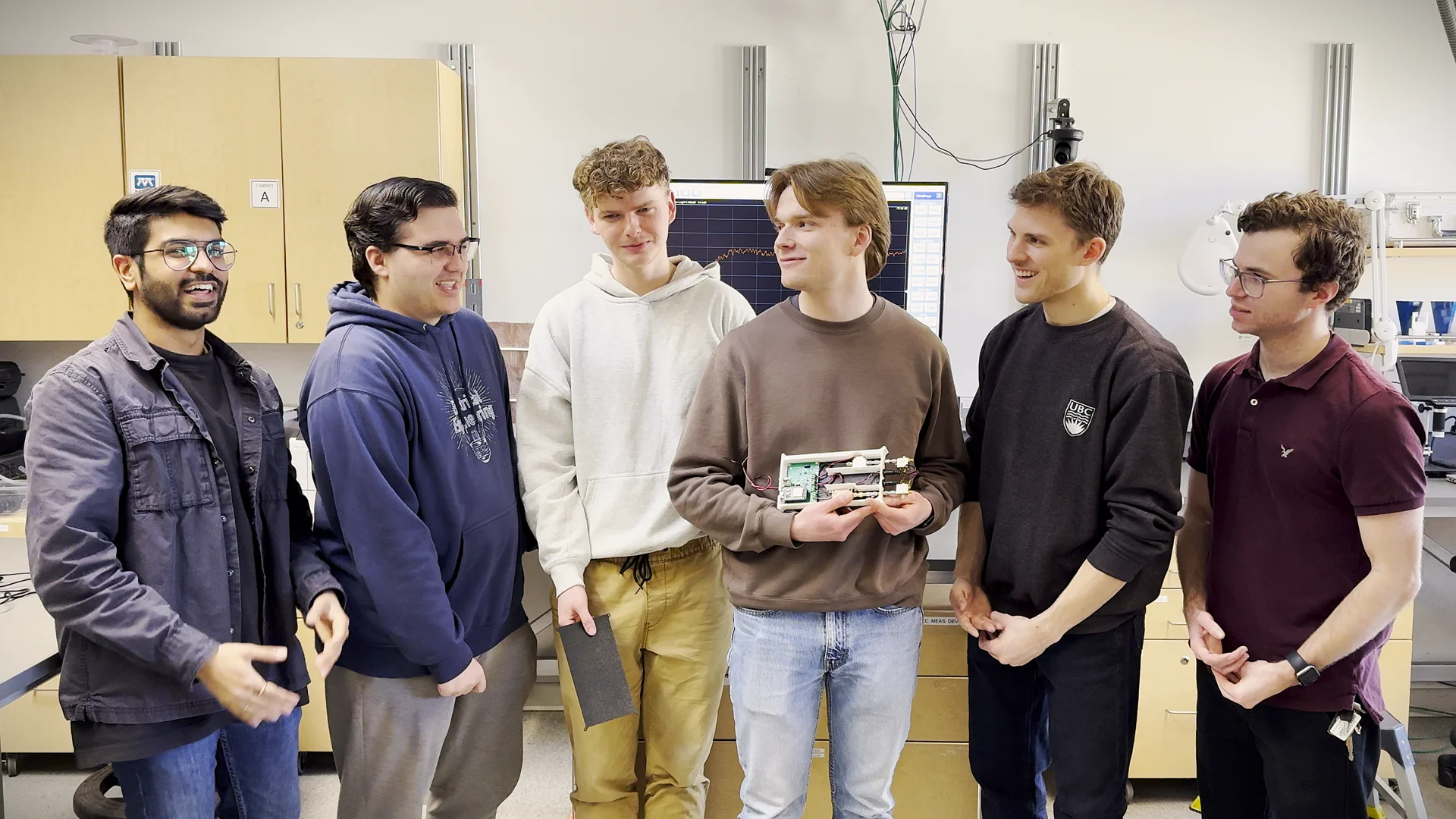
Design Process (The How)
The team was tasked with designing a scalar network analyzer (SNA) for wireless sensing and ice-detection applications. The specifications we needed to conform to were as follows:
- Operational frequency range of 10-18 GHz (Ku band)
- Dynamic range of ≥ 50 dB
- Power output of -5 dBm
- Measurement resolution of 32 sample points over range
- Low power & portable optimization (battery operated)
The key challenges were achieving the desired operational frequency range while maintaining moderate dynamic range.
What is an SNA?
A scalar network analyzer is a device that will output a sinusoid wave that is swept over a defined frequency range, and measures the amplitude response of a device under test (DUT). This response allows users to see the magnitude frequency response of a device, which in our case allows us to measure microwave ice detection sensors.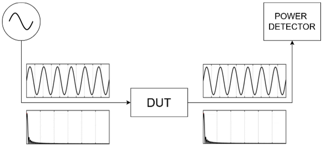
Proposed Approaches
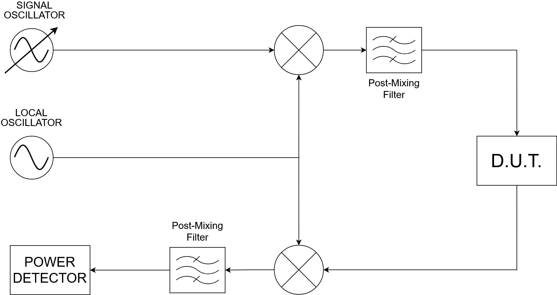
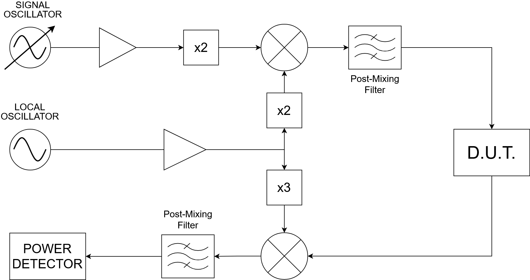
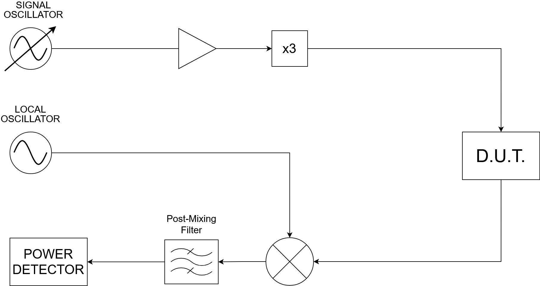
To design this SNA the team focused on the devices RF structure. I was personally tasked with developing the RF subsystems in such a way that there were options balancing performance, cost, and complexity. Design 1 This design utilizes only a voltage controlled oscillator (VCO) and power detector. Design 2 This design utilizes a double conversion methodology incorporating frequency mixing and filtering. Design 3 This design expands on the double conversion methodology by adding frequency multipliers and amplifiers for additional range and flexibility. Design 4 This design utilizes frequency multiplication at its output and a down-conversion stage at its input to make it flexible yet simple.
Initial Prototype
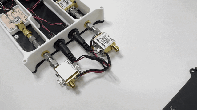
Given the timeline constraints of this project, we decided to proceed with the first design, utilizing a single VCO and power detector. We opted to use connectorized RF components to reduce any possible troubleshooting time in the future. The two major RF components we used were the HMC733 VCO by Analog Devices and the ZV47-K44RMS+ Power Detector from Mini-Circuits.
With these building blocks, the team began working on the device. We used an ESP32 microcontroller in addition to a number of components for power distribution and amplification. A printed circuit board (PCB) was developed to host all the power regulators and voltage conversion stages. The resulting unit was not glamorous, but it demonstrated the projects feasibility.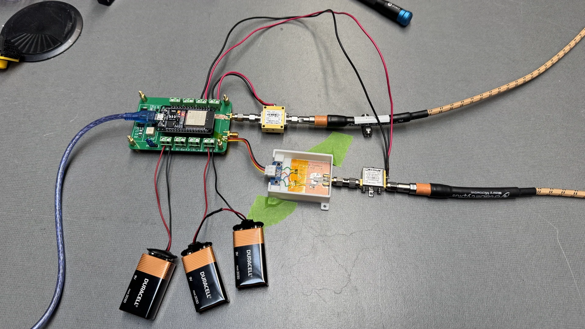
In addition to the VCO and power detector, we used two Mini-Circuits ZX60-R5183P+ amplifiers (approx. 8 dB gain). These amplifiers were used for wireless measurements using horn antennas.
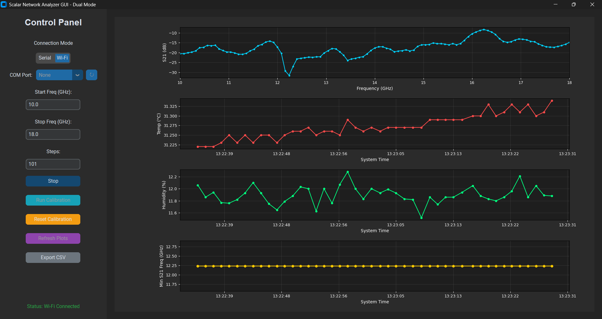
Improvements to the software
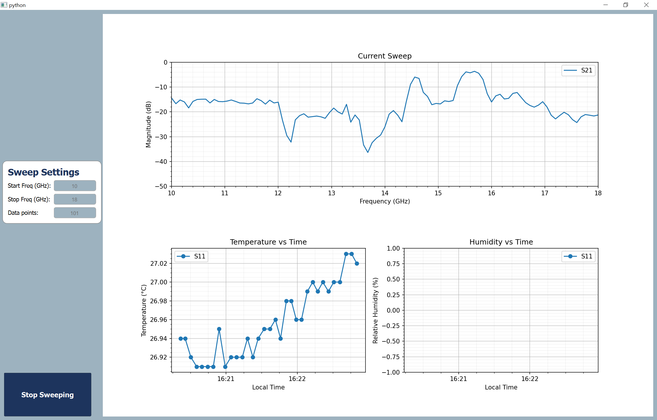
With the first prototype built, a simple graphical user interface (GUI) was designed. There were a number of iterations that this software went through. The members working on the software were Supreet, Duncan, and Aiden. First UI Revision The first GUI designed was barebones and made to function-test the first prototype. Second UI Revision The second GUI was a polished version of the first, with more attention to the design and user experience. Third UI Revision The final GUI incorporated all the features the team set out to include.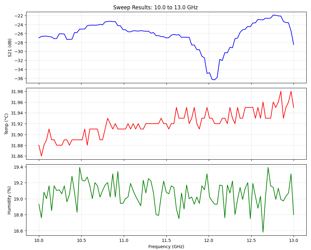
Final Design
With the results we were achieving, we looked into areas of our design we could improve. Two distinct areas of improvement we discovered were power consumption and user experience.
New PCB
A new PCB was designed for the device to incorporate new power distribution networks. I was tasked with designing the second PCB iteration which meant designing a new power supply for the device.
We wanted to be able to intelligently control the devices power distribution to optimize for power consumption. To do so, I incorporated a switch-mode power supply to provide the ESP32 with 3.3V, and a switch-mode power supply to provide the 18V required for tuning the VCO. To power the RF components such as the power detector, amplifiers, and VCO, I utilized linear regulators with an Enable/Disable feature for a smooth DC output that I can turn on and off using the ESP32.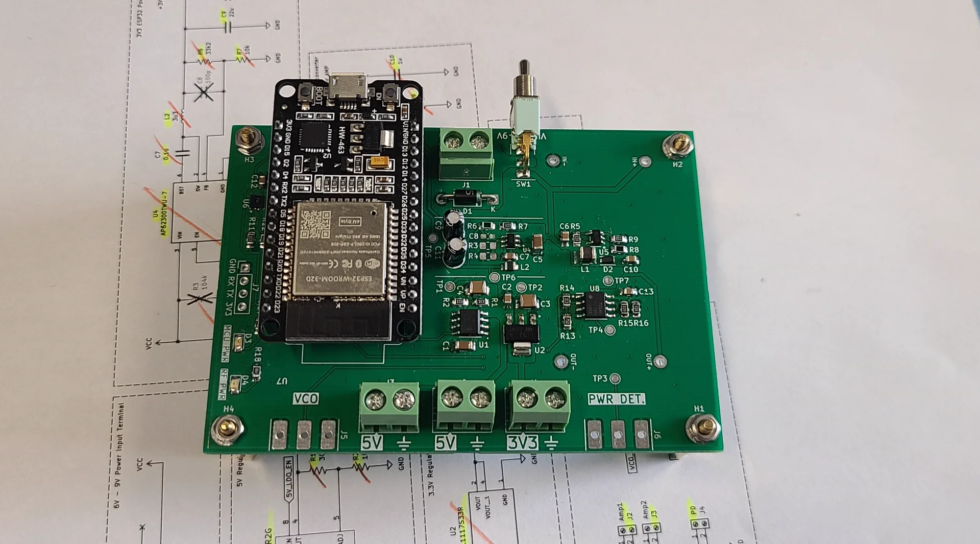
Enclosure
We achieved an improved user experience for the final design's software as shown in UI Iteration 3, but we also worked to improve the devices presentation as well. An enclosure was designed by Mathew, Aiden, and Radu, to incorporate all the components while keeping the dimensions within the desired volume.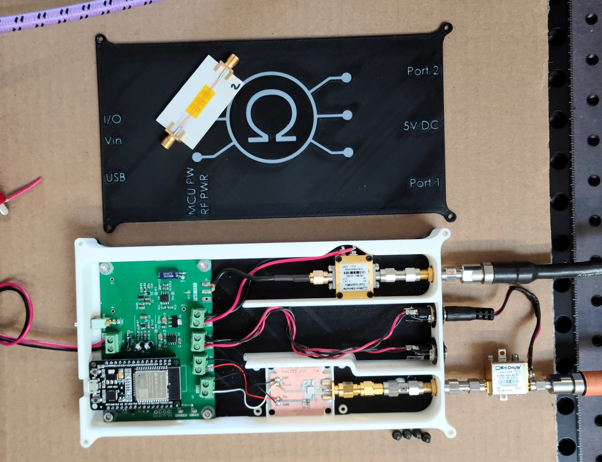
Resulting Product (The Outcome)
Closing in on the projects completion date the team conducted a final assembly of the device. The result was a product of everyones commitment, hard work, and ingenuity.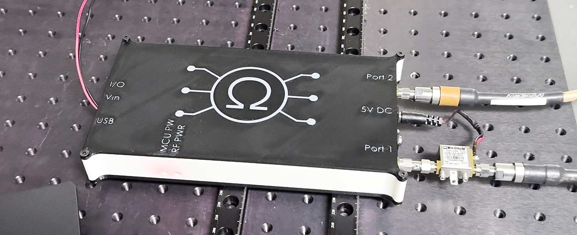
Testing
Testing the device, results showed minimal error and useable accuracy, making this device suitable for microwave sensor technologies. Below is a figure of a test done using a SRR. The blue trace shows the SRR's characteristics on a Keysight N5222B vector network analyzer which will be used as our baseline. The red trace is our SNA's measurement. Overall, the relative error between the SNA's results and the baseline was -4.34% in amplitude and +0.35% in frequency.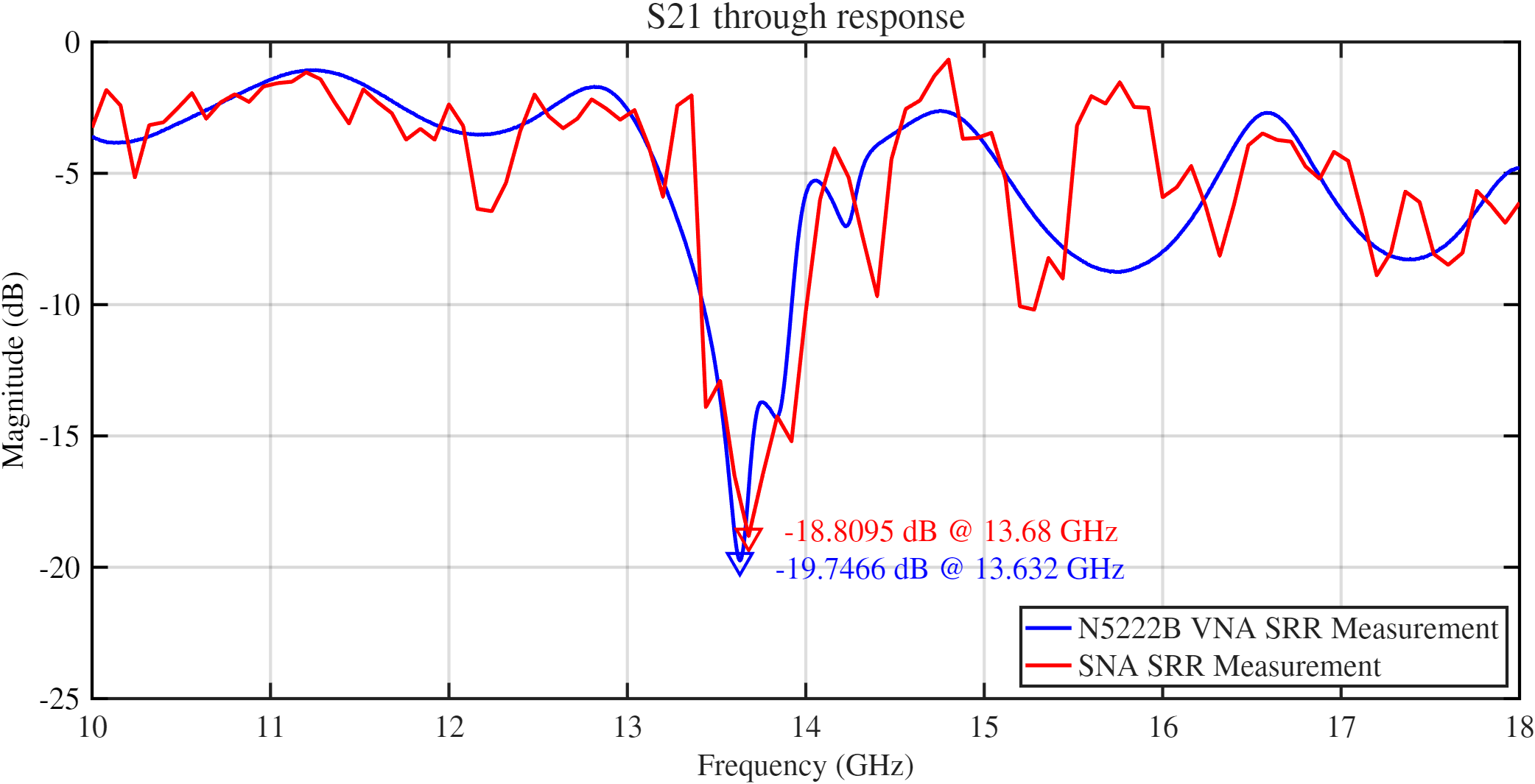
Conclusion
We successfully built a portable device that allows for microwave ice detection and sensing technology to be implemented at a lower cost. Instead of using large and expensive lab equipment, this device can be deployed in real environments like wind turbines, drones, or aircraft surfaces for ice detection applications that will provide improve safety.
Final Video Presentation
The final video presentation of our device: